|
|
|
PDF LX8386B-33CDT Data sheet ( Hoja de datos )
| Número de pieza | LX8386B-33CDT | |
| Descripción | 1.5 A LOW DROPOUT POSITIVE REGULATORS | |
| Fabricantes | Microsemi Corporation | |
| Logotipo | ||
Hay una vista previa y un enlace de descarga de LX8386B-33CDT (archivo pdf) en la parte inferior de esta página. Total 7 Páginas | ||
|
No Preview Available !
L I N DO C # : 8386
LX8386-xx/8386A-xx/8386B-xx
T H E I N F I N I T E P O W E R O F I N N O VAT I O N
1.5A LOW DROPOUT POSITIVE REGULATORS
P R O D U C T I O N D ATA S H E E T
DESCRIPTION
The LX8386/86A/86B series ICs are
positive regulators designed to provide
1.5A output current. These regulators
yield higher efficiency than currently
available devices with all internal
circuitry designed to operate down to a
1V input-to-output differential. In this
product, the dropout voltage is fully
specified as a function of load current.
Dropout is guaranteed at a maximum of
1.3V (LX8386A/86B) and 1.5V (LX8386)
at maximum output current, decreasing
at lower load currents. On-chip
trimming adjusts the reference voltage
to 1% (0.8% for the 8386B) initial
accuracy and 2% (1% for the 8386B)
over line, load and temperature.
The LX8386/86A/86B series devices
are pin-compatible with earlier 3-
terminal regulators, such as 117 series
products. While a 10µF output capacitor
is required on both input and output of
these new devices, this capacitor is
generally included in most regulator
designs.
The LX8386/86A/86B series quiescent
current flows into the load, increasing
efficiency. This feature contrasts with
PNP regulators, where up to 10% of the
output current is wasted as quiescent
current. The LX8386-xxI is specified
over the full industrial temperature
range of -25°C to +125°C and the
LX8386/86A/86B-xxC is specified over
the commercial range of 0°C to +125°C.
NOTE: For current data & package dimensions, visit our web site: http://www.linfinity.com.
PRODUCT HIGHLIGHT
3.3V, 1.5A RE G U L AT O R
5V
1500µF
6MV1500GX
IN LX8386 OUT
121Ω
ADJ 1%
3.3V at 1.5A
1500µF, 6.3V
6MV1500GX
from Sanyo
KEY FEATURES
s Three-Terminal Adjustable or Fixed
Output
s Guaranteed <1.3V Headroom
at 1.5A (LX8386A/86B)
s Output Current of 1.5A Minimum
s Operates Down to 1V Dropout
p 0.015% Line Regulation
p 0.1% Load Regulation
s Evaluation Board Available:
Request LXE9001 EVALUATION KIT
A P P L I C AT I O N S
s High Efficiency Linear Regulators
s Post Regulators For Switching Power
Supplies
s Battery Chargers
s Constant Current Regulators
s ASIC & Low Voltage IC Supplies
s Memory Cards
s Graphics & Sound Chipsets
AVAILABLE O PTIONS PER PAR T #
Part #
Output
Voltage
LX8386/86A/86B-00 Adjustable
LX8386/86A/86B-33
3.3V
Other voltage options may be available —
Please contact factory for details.
200Ω
1%
PACKAGE ORDER INFORMATION
TA (°C)
Max. Ref.
Accuracy
Max. Dropout
Voltage
P
Plastic
3-pin
TO-220
DD
Plastic
3-pin
TO-263
DT
Plastic T0-252
(D-Pak) 3-pin
2.0%
1.5V
LX8386-xxCP
LX8386-xxCDD LX8386-xxCDT
0 to 125
2.0%
1.0%
1.3V
1.3V
LX8386A-xxCP
LX8386B-xxCP
LX8386A-xxCDD
LX8386B-xxCDD
LX8386A-xxCDT
LX8386B-xxCDT
-25 to 125
2.0%
1.5V
LX8386-xxIP
LX8386-xxIDD
—
Note: All surface-mount packages are available in Tape & Reel, append the letter "T" to part number. (i.e. LX8386A-xxCDDT)
"xx" refers to output voltage, please see table above.
Copyright © 1999
Rev. 1.7a 10/00
LINFINITY MICROELECTRONICS INC.
11861 WESTERN AVENUE, GARDEN GROVE, CA. 92841, 714-898-8121, FAX: 714-893-2570
1
1 page 
PRODUCT DATABOOK 1996/1997
LX8386-xx/8386A-xx/8386B-xx
1.5A LOW DROPOUT POSITIVE REGULATORS
P R O D U C T I O N D ATA S H E E T
APPLICATION NOTES
OVERLOAD RECOVERY (continued)
If this limited current is not sufficient to develop the designed
voltage across the output resistor, the voltage will stabilize at some
lower value, and will never reach the designed value. Under these
circumstances, it may be necessary to cycle the input voltage down
to zero in order to make the regulator output voltage return to
regulation.
RIPPLE REJECTION
Ripple rejection can be improved by connecting a capacitor
between the ADJ pin and ground. The value of the capacitor should
be chosen so that the impedance of the capacitor is equal in
magnitude to the resistance of R1 at the ripple frequency. The
capacitor value can be determined by using this equation:
C = 1 / (6.28 * FR * R1)
where: C ≡ the value of the capacitor in Farads;
select an equal or larger standard value.
FR ≡ the ripple frequency in Hz
R1 ≡ the value of resistor R1 in ohms
At a ripple frequency of 120Hz, with R1 = 100Ω:
C = 1 / (6.28 * 120Hz * 100Ω) = 13.3µF
The closest equal or larger standard value should be used, in this
case, 15µF.
When an ADJ pin bypass capacitor is used, output ripple
amplitude will be essentially independent of the output voltage. If
an ADJ pin bypass capacitor is not used, output ripple will be
proportional to the ratio of the output voltage to the reference
voltage:
M = VOUT/VREF
where: M ≡ a multiplier for the ripple seen when the
ADJ pin is optimally bypassed.
VREF = 1.25V.
For example, if VOUT = 2.5V the output ripple will be:
M = 2.5V/1.25V= 2
Output ripple will be twice as bad as it would be if the ADJ pin
were to be bypassed to ground with a properly selected capacitor.
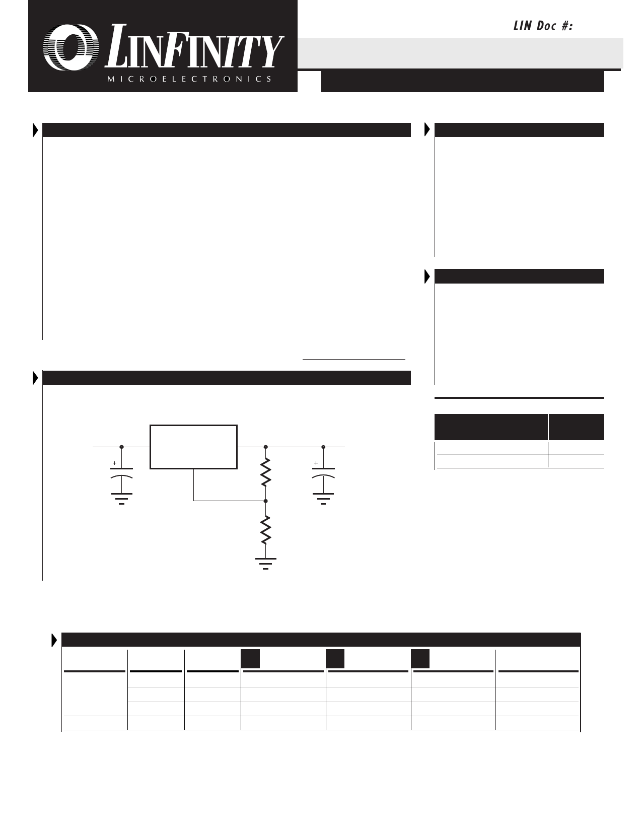
OUTPUT VOLTAGE
The LX8386/86A/86B ICs develop a 1.25V reference voltage between
the output and the adjust terminal (See Figure 2). By placing a resistor,
R1, between these two terminals, a constant current is caused to flow
through R1 and down through R2 to set the overall output voltage.
Normally this current is the specified minimum load current of 10mA.
Because IADJis very small and constant when compared with the current
through R1, it represents a small error and can usually be ignored.
LX8386/86A/86B
VIN IN OUT
ADJ
VREF
IADJ
50µA
VOUT = VREF
1
+
R2
R1
+ IADJ R2
VOUT
R1
R2
FIGURE 2 — Basic Adjustable Regulator
LOAD REGULATION
Because the LX8386/86A/86B regulators are three-terminal devices,
it is not possible to provide true remote load sensing. Load
regulation will be limited by the resistance of the wire connecting
the regulator to the load. The data sheet specification for load
regulation is measured at the bottom of the package. Negative side
sensing is a true Kelvin connection, with the bottom of the output
divider returned to the negative side of the load. Although it may
not be immediately obvious, best load regulation is obtained when
the top of the resistor divider, (R1), is connected directly to the case
of the regulator, not to the load. This is illustrated in Figure 3. If R1
were connected to the load, the effective resistance between the
regulator and the load would be:
RPeff = RP *
R2+R1
R1
where: RP ≡ Actual parasitic line resistance.
When the circuit is connected as shown in Figure 3, the parasitic
resistance appears as its actual value, rather than the higher RPeff.
LX8386/86A/86B
ParRaPsitic
Line Resistance
VIN IN
OUT
ADJ Connect
R1 to Case
of Regulator
R1
R2 RL
Connect
R2
to Load
FIGURE 3 — Connections For Best Load Regulation
Copyright © 1999
Rev. 1.7a 10/00
5
5 Page | ||
| Páginas | Total 7 Páginas | |
| PDF Descargar | [ Datasheet LX8386B-33CDT.PDF ] | |
Hoja de datos destacado
| Número de pieza | Descripción | Fabricantes |
| LX8386B-33CDD | 1.5 A LOW DROPOUT POSITIVE REGULATORS | Microsemi Corporation |
| LX8386B-33CDT | 1.5 A LOW DROPOUT POSITIVE REGULATORS | Microsemi Corporation |
| Número de pieza | Descripción | Fabricantes |
| SLA6805M | High Voltage 3 phase Motor Driver IC. |
Sanken |
| SDC1742 | 12- and 14-Bit Hybrid Synchro / Resolver-to-Digital Converters. |
Analog Devices |
|
DataSheet.es es una pagina web que funciona como un repositorio de manuales o hoja de datos de muchos de los productos más populares, |
| DataSheet.es | 2020 | Privacy Policy | Contacto | Buscar |