|
|
|
PDF DAC312 Data sheet ( Hoja de datos )
| Número de pieza | DAC312 | |
| Descripción | 12-Bit High Speed Multiplying D/A Converter | |
| Fabricantes | Analog Devices | |
| Logotipo | ||
Hay una vista previa y un enlace de descarga de DAC312 (archivo pdf) en la parte inferior de esta página. Total 14 Páginas | ||
|
No Preview Available !
a
FEATURES
Differential Nonlinearity: ؎1/2 LSB
Nonlinearity: 0.05%
Fast Settling Time: 250 ns
High Compliance: –5 V to +10 V
Differential Outputs: 0 to 4 mA
Guaranteed Monotonicity: 12 Bits
Low Full-Scale Tempco: 10 ppm/؇C
Circuit Interface to TTL, CMOS, ECL, PMOS/NMOS
Low Power Consumption: 225 mW
Industry Standard AM6012 Pinout
Available In Die Form
12-Bit High Speed Multiplying
D/A Converter
DAC312
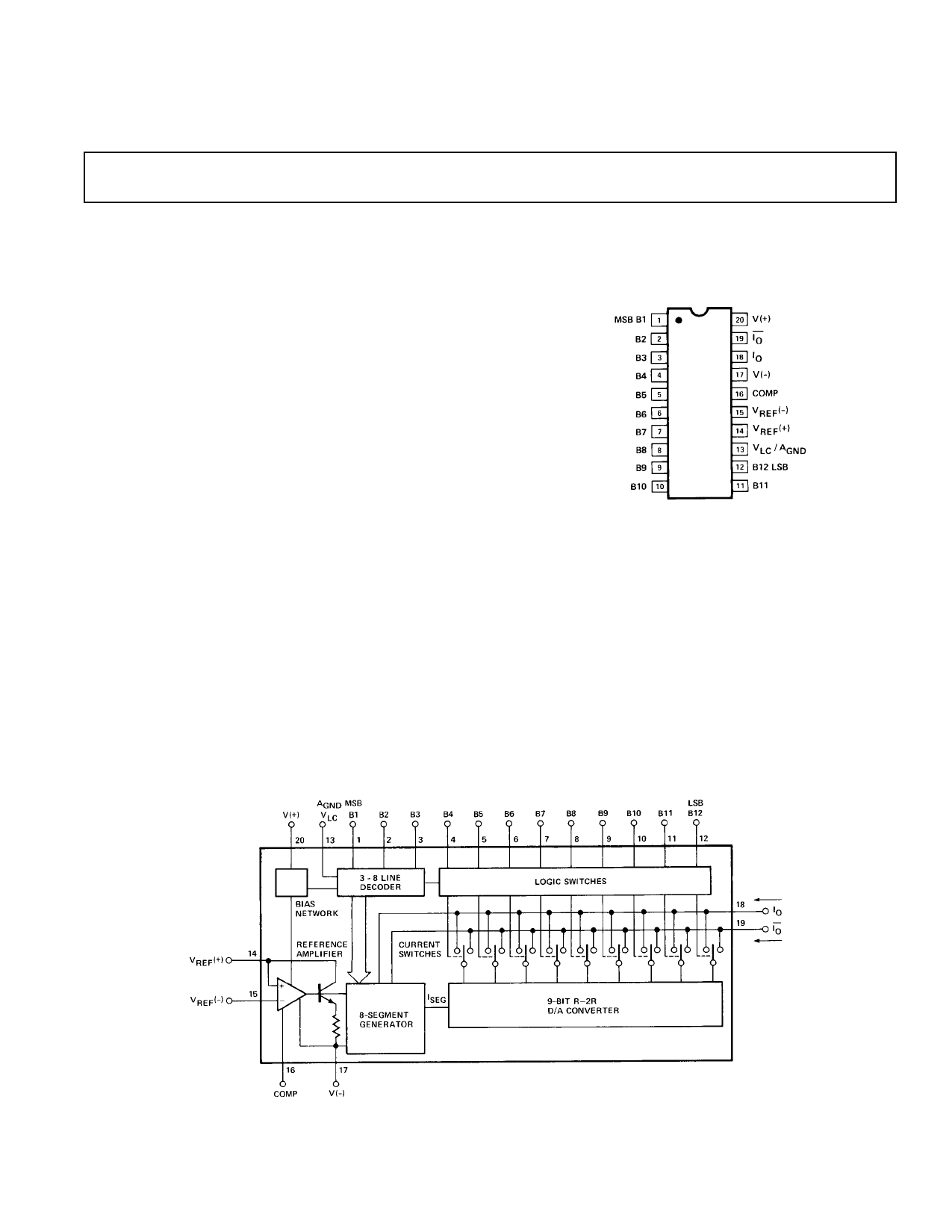
PIN CONNECTIONS
20-Pin Hermetic DIP (R-Suffix),
20-Pin Plastic DIP (P-Suffix),
20-Pin SOL (S-Suffix)
GENERAL DESCRIPTION
The DAC312 series of 12-bit multiplying digital-to-analog con-
verters provide high speed with guaranteed performance to
0.012% differential nonlinearity over the full commercial oper-
ating temperature range.
High compliance and low drift characteristics (as low as
The DAC312 combines a 9-bit master D/A converter with a
3-bit (MSBs) segment generator to form an accurate 12-bit D/A
converter at low cost. This technique guarantees a very uniform
step size (up to ± 1/2 LSB from the ideal), monotonicity to
12-bits and integral nonlinearity to 0.05% at its differential cur-
rent outputs. In order to provide the same performance with a
10 ppm/°C) are also features of the DAC312 along with an ex-
cellent power supply rejection ratio of ± .001% FS/%∆V. Oper-
ating over a power supply range of +5/–11 V to ± 18 V the
device consumes 225 mW at the lower supply voltages with an
absolute maximum dissipation of 375 mW at the higher supply
levels.
12-bit R-2R ladder design, an integral nonlinearity over tem-
perature of 1/2 LSB (0.012%) would be required.
With their guaranteed specifications, single chip reliability and
low cost, the DAC312 device makes excellent building blocks
The 250 ns settling time with low glitch energy and low power
consumption are achieved by careful attention to the circuit de-
sign and stringent process controls. Direct interface with all
popular logic families is achieved through the logic threshold
for A/D converters, data acquisition systems, video display driv-
ers, programmable test equipment and other applications where
low power consumption and complete input/output versatility
are required.
terminal.
FUNCTIONAL BLOCK DIAGRAM
REV. C
Information furnished by Analog Devices is believed to be accurate and
reliable. However, no responsibility is assumed by Analog Devices for its
use, nor for any infringements of patents or other rights of third parties
which may result from its use. No license is granted by implication or
otherwise under any patent or patent rights of Analog Devices.
© Analog Devices, Inc., 1996
One Technology Way, P.O. Box 9106, Norwood, MA 02062-9106, U.S.A.
Tel: 617/329-4700
Fax: 617/326-8703
1 page 
ABSOLUTE MAXIMUM RATINGS1
Operating Temperature
DAC312E . . . . . . . . . . . . . . . . . . . . . . . . . . . . . . 0°C to +70°C
DAC312F, DAC312H . . . . . . . . . . . . . . . . . . –40°C to +85°C
Junction Temperature . . . . . . . . . . . . . . . . . . . . –65°C to +150°C
Storage Temperature (Tj) . . . . . . . . . . . . . . . . . –65°C to +125°C
Lead Temperature (Soldering, 60 sec) . . . . . . . . . . . . . . . . 300°C
Power Supply Voltage . . . . . . . . . . . . . . . . . . . . . . . . . . . . . ± 18 V
Logic Inputs . . . . . . . . . . . . . . . . . . . . . . . . . . . . . –5 V to +18 V
Analog Current Outputs . . . . . . . . . . . . . . . . . . . . –8 V to +12 V
Reference Inputs V14, V15 . . . . . . . . . . . . . . . . . . . . . . . V– to V+
Reference Input Differential Voltage (V14, V15) . . . . . . . . . . ± 18 V
Reference Input Current (I14) . . . . . . . . . . . . . . . . . . . . . 1.25 mA
Package Type
JA2
JC
Units
20-Pin Hermetic DIP (R)
20-Pin Plastic DIP (P)
20-Pin SOL (S)
76
69
88
11
27
25
°C/W
°C/W
°C/W
NOTES
1Absolute maximum ratings apply to both DICE and packaged parts, unless
otherwise noted.
2θJA is specified for worst case mounting conditions, i.e., θJA is specified for device
in socket for cerdip and P-DIP packages; θJA is specified for device soldered to
printed circuit board for SOL package.
DAC312
ORDERING GUIDE1
Model
DNL
Temperature
Range
Package
Package
Description Option
DAC312ER2 ± 1/2 LSB 0°C to +70°C
Cerdip-20
Q-20
DAC312FR
± 1 LSB –40°C to +85°C Cerdip-20
Q-20
DAC312BR/883 ± 1 LSB –55°C to +125°C Cerdip-20 Q-20
DAC312HP ± 1 LSB –40°C to +85°C Plastic DIP-20 N-20
DAC312HS ± 1 LSB –40°C to +85°C SOL-20
R-20
NOTES
1Burn-in is available on commercial and industrial temperature range parts in
cerdip, plastic DIP, and TO-can packages.
2For devices processed in total compliance to MIL-STD-883, add/883 after part
number. Consult factory for 883 data sheet.
CAUTION
ESD (electrostatic discharge) sensitive device. Electrostatic charges as high as 4000 V readily
accumulate on the human body and test equipment and can discharge without detection.
Although the DAC312 features proprietary ESD protection circuitry, permanent damage may
occur on devices subjected to high energy electrostatic discharges. Therefore, proper ESD
precautions are recommended to avoid performance degradation or loss of functionality.
WARNING!
ESD SENSITIVE DEVICE
REV. C
–5–
5 Page 
DAC312
ANALOG OUTPUT CURRENTS
Both true and complemented output sink currents are provided
where IO + IO = IFR. Current appears at the true output when a
“1” is applied to each logic input. As the binary count increases,
the sink current at pin 18 increases proportionally, in the fash-
ion of a “positive logic” D/A converter. When a “0” is applied to
any input bit, that current is turned off at pin 18 and turned on
at pin 19. A decreasing logic count increases IO as in a negative
or inverted logic D/A converter. Both outputs may be used si-
multaneously. If one of the outputs is not required it must still
be connected to ground or to a point capable of sourcing IFR; do
not leave an unused output pin open.
Both outputs have an extremely wide voltage compliance en-
abling fast direct current-to-voltage conversion through a resis-
tor tied to ground or other voltage source. Positive compliance
is 25 V above V– and is independent of the positive supply.
Negative compliance is +10 V above V–.
The dual outputs enable double the usual peak-to-peak load
swing when driving loads in quasi-differential fashion. This fea-
ture is especially useful in cable driving, CRT deflection and in
other balanced applications such as driving center-tapped coils
and transformers.
POWER SUPPLIES
The DAC312 operates over a wide range of power supply volt-
ages from a total supply of 20 V to 36 V. When operating with
V– supplies of –10 V or less, IREF ≤ 1 mA is recommended. Low
reference current operation decreases power consumption and
increases negative compliance, reference amplifier negative
common-mode range, negative logic input range, and negative
logic threshold range; consult the various figures for guidance.
For example, operation at –9 V with IREF = 1 mA is not recom-
mended because negative output compliance would be reduced
to near zero. Operation from lower supplies is possible, however
at least 8 V total must be applied to insure turn-on of the inter-
nal bias network.
Symmetrical supplies are not required, as the DAC312 is quite
insensitive to variations in supply voltage. Battery operation is
feasible as no ground connection is required; however, an artifi-
cial ground may be used to insure logic swings, etc. remain be-
tween acceptable limits.
TEMPERATURE PERFORMANCE
The nonlinearity and monotonicity specifications of the
DAC312 are guaranteed to apply over the entire rated operating
temperature range. Full-scale output current drift is tight, typi-
cally ± 10 ppm/°C, with zero-scale output current and drift es-
sentially negligible compared to 1/2 LSB.
The temperature coefficient of the reference resistor R14 should
match and track that of the output resistor for minimum overall
full-scale drift. Settling times of the DAC312 decrease approxi-
mately 10% at –55°C; at +125°C an increase of about 15% is
typical.
SETTLING TIME
The DAC312 is capable of extremely fast settling times; typi-
cally 250 ns at IREF = 1.0 mA. Judicious circuit design and care-
ful board layout must be employed to obtain full performance
potential during testing and application. The logic switch design
enables propagation delays of only 25 ns for each of the 12 bits.
Settling time to within 1/2 LSB of the LSB is therefore 25 ns,
with each progressively larger bit taking successively longer. The
MSB settles in 250 ns, thus determining the overall settling time
of 250 ns. Settling to 10-bit accuracy requires about 90 ns to
130 ns. The output capacitance of the DAC312 including the
package is approximately 20 pF; therefore, the output RC time
constant dominates settling time if RL > 500 Ω.
Settling time and propagation delay are relatively insensitive to
logic input amplitude and rise and fall times, due to the high
gain of the logic switches. Settling time also remains essentially
constant for IREF values down to 0.5 mA, with gradual increases
for lower IREF values lies in the ability to attain a given output
level with lower load resistors, thus reducing the output RC
time constant.
Measurement of the settling time requires the ability to accu-
rately resolve ± 1/2 LSB of current, which is ± 500 nA for 4 mA
FSR. In order to assure the measurement is of the actual settling
time and not the RC time of the output network, the resistive
termination on the output of the DAC must be 500 Ω or less.
This does, however, place certain limitations on the testing ap-
paratus. At IREF values of less than 0.5 mA, it is difficult to pre-
vent RC damping of the output and maintain adequate
sensitivity. Because the DAC312 has 8 equal current sources for
the 3 most significant bits, the major carry occurs at the code
change of 000111111111 to 111000000000. The worst case set-
tling time occurs at the zero to full-scale transition and it re-
quires 9.2 time constants for the DAC output to settle to within
± 1/2 LSB (0.0125%) of its final value.
The DAC312 switching transients or “glitches” are on the order
of 500 mV-ns. This is most evident when switching through the
major carry and may be further reduced by adding small capaci-
tive loads at the output with a minor sacrifice in transition speeds.
Fastest operation can be obtained by using short leads, minimiz-
ing output capacitance and load resistor values, and by adequate
bypassing at the supply, reference, and VLC terminals. Supplies
do not require large electrolytic bypass capacitors as the supply
current drain is independent of input logic states; 0.1 µF capaci-
tors at the supply pins provide full transient protection.
REV. C
–11–
11 Page | ||
| Páginas | Total 14 Páginas | |
| PDF Descargar | [ Datasheet DAC312.PDF ] | |
Hoja de datos destacado
| Número de pieza | Descripción | Fabricantes |
| DAC312 | 12-Bit High Speed Multiplying D/A Converter | Analog Devices |
| DAC3151 | DAC31x1 Single 14-12- and 10-Bit 500-MSPS Digital-to-Analog Converters (Rev. B) | Texas Instruments |
| DAC3161 | DAC31x1 Single 14-12- and 10-Bit 500-MSPS Digital-to-Analog Converters (Rev. B) | Texas Instruments |
| DAC3162 | DUAL-CHANNEL 10-/12-BIT 500 MSPS DIGITAL-TO-ANALOG CONVERTERS (DACs) (Rev. D) | Texas Instruments |
| Número de pieza | Descripción | Fabricantes |
| SLA6805M | High Voltage 3 phase Motor Driver IC. |
Sanken |
| SDC1742 | 12- and 14-Bit Hybrid Synchro / Resolver-to-Digital Converters. |
Analog Devices |
|
DataSheet.es es una pagina web que funciona como un repositorio de manuales o hoja de datos de muchos de los productos más populares, |
| DataSheet.es | 2020 | Privacy Policy | Contacto | Buscar |