|
|
|
PDF DAC8413 Data sheet ( Hoja de datos )
| Número de pieza | DAC8413 | |
| Descripción | 12-Bit DAC Voltage Output | |
| Fabricantes | Analog Devices | |
| Logotipo | ||
Hay una vista previa y un enlace de descarga de DAC8413 (archivo pdf) en la parte inferior de esta página. Total 20 Páginas | ||
|
No Preview Available !
Data Sheet
FEATURES
+5 V to ±15 V operation
Unipolar or bipolar operation
True voltage output
Double-buffered inputs
Reset to minimum (DAC8413) or center scale (DAC8412)
Fast bus access time
Readback
APPLICATIONS
Automatic test equipment
Digitally controlled calibration
Servo controls
Process control equipment
GENERAL DESCRIPTION
The DAC8412/DAC8413 are quad, 12-bit voltage output
DACs with readback capability. Built using a complementary
BiCMOS process, these monolithic DACs offer the user very
high package density.
Output voltage swing is set by the two reference inputs VREFH
and VREFL. By setting the VREFL input to 0 V and VREFH to a
positive voltage, the DAC provides a unipolar positive output
range. A similar configuration with VREFH at 0 V and VREFL at a
negative voltage provides a unipolar negative output range.
Bipolar outputs are configured by connecting both VREFH and
VREFL to nonzero voltages. This method of setting output voltage
range has advantages over other bipolar offsetting methods
because it is not dependent on internal and external resistors
with different temperature coefficients.
Digital controls allow the user to load or read back data from any
DAC, load any DAC, and transfer data to all DACs at one time.
An active low RESET loads all DAC output registers to midscale
for the DAC8412 and zero scale for the DAC8413.
The DAC8412/DAC8413 are available in 28-lead plastic DIP,
28-lead ceramic DIP, 28-lead PLCC, and 28-lead LCC packages.
Quad, 12-Bit DAC
Voltage Output with Readback
DAC8412/DAC8413
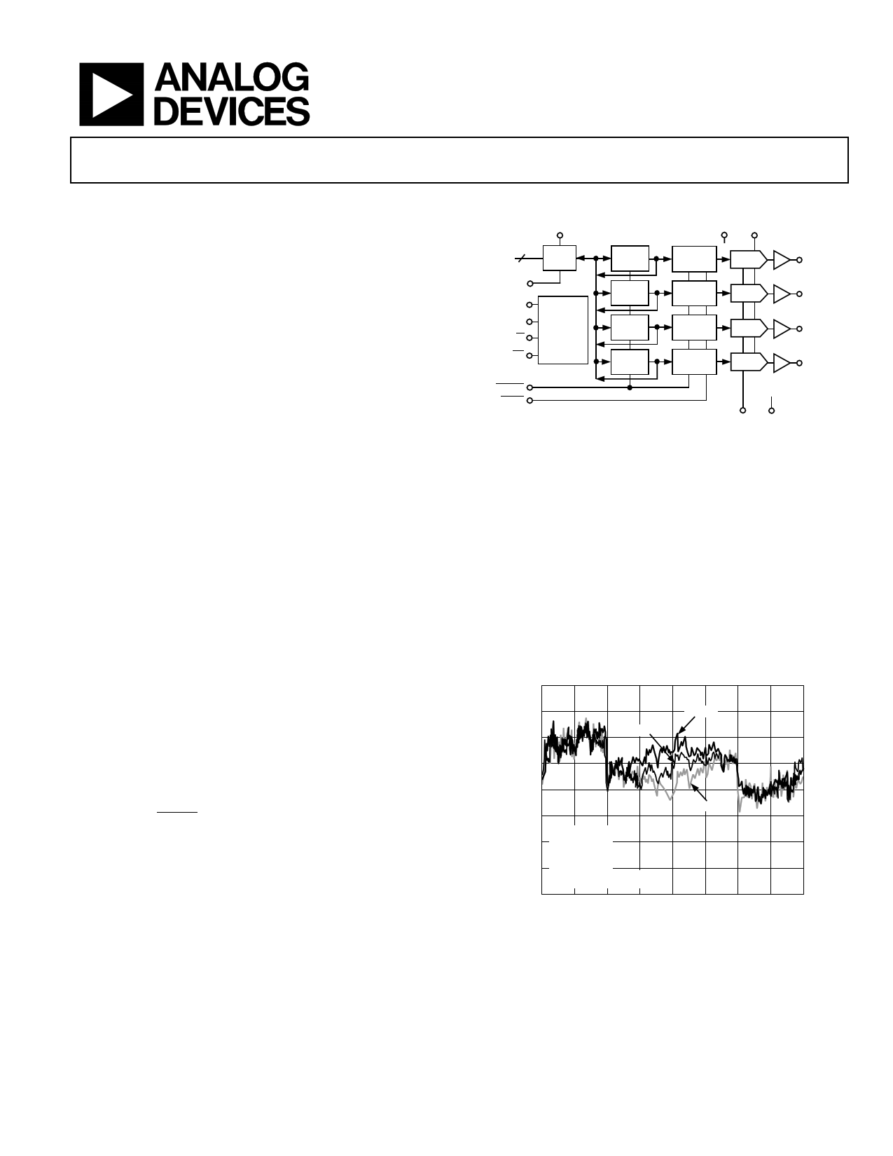
FUNCTIONAL BLOCK DIAGRAM
VLOGIC
VDD VREFH
DATA 12
I/O
DGND
I/O
PORT
A0
A1
CONTROL
R/W
LOGIC
CS
INPUT
REG A
INPUT
REG B
INPUT
REG C
INPUT
REG D
OUTPUT
REG A
OUTPUT
REG B
OUTPUT
REG C
OUTPUT
REG D
DAC A
DAC B
DAC C
DAC D
RESET
LDAC
Figure 1.
VREFL VSS
VOUTA
VOUTB
VOUTC
VOUTD
They can be operated from a wide variety of supply and reference
voltages with supplies ranging from single +5 V to ±15 V, and
references from +2.5 V to ±10 V. Power dissipation is less than
330 mW with ±15 V supplies and only 60 mW with a +5 V supply.
For MIL-STD-883 applications, contact your local Analog
Devices, Inc. sales office for the DAC8412/DAC8413/883 data
sheet, which specifies operation over the −55°C to +125°C
temperature range. All 883 parts are also available on Standard
Military Drawings 5962-91 76401MXA through 76404M3A.
0.500
0.375
0.250
+25°C
+125°C
0.125
0
–0.125
–55°C
–0.250
–0.375
–0.500
0
VDD = +15V
VSS = –15V
VREFH = +10V
VREFL = –10V
TA = –55°C, +25°C, +125°C
512 1024 1536 2046 2548 2560
DIGITAL INPUT CODE (Decimal)
3072
Figure 2. INL vs. Code Over Temperature
4096
Rev. G
Document Feedback
Information furnished by Analog Devices is believed to be accurate and reliable. However, no
responsibilityisassumedbyAnalogDevices for itsuse,nor foranyinfringementsofpatentsor other
rights of third parties that may result from its use. Specifications subject to change without notice. No
license is granted by implication or otherwise under any patent or patent rights of Analog Devices.
Trademarksandregisteredtrademarksarethepropertyoftheirrespectiveowners.
One Technology Way, P.O. Box 9106, Norwood, MA 02062-9106, U.S.A.
Tel: 781.329.4700 ©2000–2013 Analog Devices, Inc. All rights reserved.
Technical Support
www.analog.com
1 page 
Data Sheet
DAC8412/DAC8413
Parameter
Write Data Setup
Write Data Hold
Load Data Pulse Width
Reset Pulse Width
Chip Select Read Pulse Width
Read Data Hold
Read Data Setup
Data to High-Z
Chip Select to Data
SUPPLY CHARACTERISTICS
Power Supply Sensitivity
Positive Supply Current
Negative Supply Current
Power Dissipation
Symbol
tWDS
tWDH
tLDW
tRESET
tRCS
tRDH
tRDS
tDZ
tCSD
Conditions
tWCS = 150 ns
tWCS = 150 ns
tRCS = 170 ns
tRCS = 170 ns
CL = 10 pF
CL = 100 pF
PSS
IDD
ISS
PDISS
VSS = −5.0 V
VSS = 0 V
VSS = −5.0 V
Min Typ
20
0
180
150
170
20
0
100
7
−10
60
110
1 All supplies can be varied ±5%, and operation is guaranteed. Device is tested with VDD = 4.75 V.
2 For single-supply operation only (VREFL = 0.0 V, VSS = 0.0 V). Due to internal offset errors, INL and DNL are measured beginning at 0x005.
3 Operation is guaranteed over this reference range, but linearity is neither tested nor guaranteed.
4 All parameters are guaranteed by design.
5 All input control signals are specified with tr = tf = 5 ns (10% to 90% of 5 V) and timed from a voltage level of 1.6 V.
Max
200
320
12
Units
ns
ns
ns
ns
ns
ns
ns
ns
ns
ppm/V
mA
mA
mW
mW
CS
R/W
A0/A1
DATA
OUT
tRCS
tRDS
tRDH
tAS tAH
HIGH-Z
DATA VALID
tDZ
HIGH-Z
tCSD
Figure 3. Data Output (Read Timing)
CS
R/W
A0/A1
tWS
tAS
tWCS
tWH
tAH
LDAC
DATA IN
tLS
tWDS
tLH tLDW
tWDH
RESET
tRESET
Figure 4. Data Write (Input and Output Registers) Timing
Rev. G | Page 5 of 20
5 Page 
Data Sheet
10V
1V/DIV
EA
TRIG'D
0V
–580ns
15.5mV
0
INPUT
–5V
2mV/DIV
5V/DIV
TRIG'D
VDD = +15V
VSS = –15V
VREFH = +10V
VREFL = –10V
TA = 25°C
1µs/DIV
Figure 22. Positive Slew Rate
9.42µs
VDD = +15V
VSS = –15V
VREFH = +10V
VREFL = –10V
TA = 25°C
–4.5mV
–1.96µs
32.5mV
5V
INPUT
0
2µs/DIV
Figure 23. Settling Time (Negative)
18.04µs
5mV/DIV
5V/DIV
TRIG'D
–17.5mV
–1.96µs
1 LSB ERROR BAND
2µs/DIV
VDD = +15V
VSS = –15V
VREFH = +10V
VREFL = –10V
TA = 25°C
18.04µs
Figure 24. Settling Time (Positive)
DAC8412/DAC8413
10V
1V/DIV
EA
TRIG'D
VDD = +15V
VSS = –15V
VREFH = +10V
VREFL = –10V
TA = 25°C
0V
–580ns
1µs/DIV
Figure 25. Negative Slew Rate
2.0 VDD = +15V
VSS = –15V
VREFH = +10V
1.5 VREFL = –10V
TA = 25°C
1.0
9.42µs
0.5
0
–0.5
0
511 1023 1535 2047 2559 3071 3583 4095
DIGITAL INPUT CODE (Decimal)
Figure 26. IVREFH vs. Code
1.0
VDD = +15V
VSS = –15V
0.8 VREFH = +10V
VREFL = –10V
TA = 25°C
0.6
0.4
0.2
0
–0.2
0.01
0.1 1
10
LOAD RESISTANCE (kΩ)
Figure 27. INL vs. Load Resistance
100
Rev. G | Page 11 of 20
11 Page | ||
| Páginas | Total 20 Páginas | |
| PDF Descargar | [ Datasheet DAC8413.PDF ] | |
Hoja de datos destacado
| Número de pieza | Descripción | Fabricantes |
| DAC8411 | DAC8x11 2-V to 5.5-V 80- A 14- and 16-Bit Low-Power Single-Channel Digital-to-Analog Converters in SC70 Package (Rev. C) | Texas Instruments |
| DAC8412 | 12-Bit DAC Voltage Output | Analog Devices |
| DAC8413 | 12-Bit DAC Voltage Output | Analog Devices |
| Número de pieza | Descripción | Fabricantes |
| SLA6805M | High Voltage 3 phase Motor Driver IC. |
Sanken |
| SDC1742 | 12- and 14-Bit Hybrid Synchro / Resolver-to-Digital Converters. |
Analog Devices |
|
DataSheet.es es una pagina web que funciona como un repositorio de manuales o hoja de datos de muchos de los productos más populares, |
| DataSheet.es | 2020 | Privacy Policy | Contacto | Buscar |