|
|
PDF HMP8171CN Data sheet ( Hoja de datos )
| Número de pieza | HMP8171CN | |
| Descripción | NTSC/PAL Video Encoder | |
| Fabricantes | Intersil Corporation | |
| Logotipo |  |
|
Hay una vista previa y un enlace de descarga de HMP8171CN (archivo pdf) en la parte inferior de esta página. Total 30 Páginas | ||
|
No Preview Available !
HMP8170, HMP8171, HMP8172, HMP8173
Data Sheet
May 1999
File Number 4284.5
NTSC/PAL Video Encoder
The HMP8170, HMP8171, HMP8172, and HMP8173 NTSC
and PAL encoders are designed for use in systems requiring
the generation of high-quality NTSC and PAL video.
YCbCr digital video data drive the P0-P15 inputs. The Y data
is optionally lowpass filtered to 6MHz and drives the Y analog
output. Cb and Cr are each lowpass filtered to 1.3MHz,
quadrature modulated, and added together. The result drives
the C analog output. The digital Y and C data are also added
together and drive the two composite analog outputs.
The DACs can drive doubly-terminated (37.5Ω) lines, and
run at a 2x oversampling rate to simplify the analog output
filter requirements.
Applications
• DVD Players
• Video CD Players
• Digital VCRs
• Multimedia PCs
Related Products
• NTSC/PAL Encoders
- HMP8154, HMP8156A
• NTSC/PAL Decoders
- HMP8115
Features
• (M) NTSC and (B, D, G, H, I, M, N, NC) PAL Operation
• BT.601 and Square Pixel Operation
• Digital Input Formats
- 8-bit, 16-bit 4:2:2 YCbCr
- 8-bit BT.656
• Analog Output Formats
- Y/C + Two Composite
- RGB + Composite
- YUV + Composite
• Flexible Video Timing Control
- Timing Master or Slave
- Selectable Polarity on Each Control Signal
- Programmable Blank Output Timing
• “Sliced” VBI Data Support
- Closed Captioning
- Widescreen Signalling (WSS)
- BT.653 System B and C Teletext
- NABTS (North American Broadcast Teletext)
- WST (World System Teletext)
• Four 2x Oversampling, 10-Bit DACs
• Fast I2C Interface
Ordering Information
PART NUMBER
MACROVISION
v7.01
RGB / YUV
OUTPUTS
TEMP. RANGE
(oC)
PACKAGE
PKG. NO.
HMP8170CN
no
no
0 to 70
64 Ld PQFP (Note 2) Q64.14x14
HMP8171CN (Note 1)
yes
no
0 to 70
64 Ld PQFP (Note 2) Q64.14x14
HMP8172CN
no
yes
0 to 70
64 Ld PQFP (Note 2) Q64.14x14
HMP8173CN (Note 1)
yes
yes
0 to 70
64 Ld PQFP (Note 2) Q64.14x14
HMP817xEVAL1
Daughter Card Evaluation Platform, where x is replaced by 0, 1, 2, or 3 (Note 3).
NOTES:
1. The HMP8171 and HMP8173 may be purchased by Macrovision Authorized Buyers only. These devices are protected by U.S. patent numbers
4,631,603, 4,577,216, and 4,819,098, and other intellectual property rights. The use of Macrovision’s copy protection technology in the devices
must be authorized by Macrovision and is intended for home and other limited pay-per-view uses only, unless otherwise authorized in writing
by Macrovision. Reverse engineering or disassembly is prohibited.
2. PQFP is also known as QFP and MQFP.
3. Evaluation board descriptions are in the Applications section.
1 CAUTION: These devices are sensitive to electrostatic discharge; follow proper IC Handling Procedures.
Intercast™ is a trademark of Intel Corporation.
http://www.intersil.com or 407-727-9207 | Copyright © Intersil Corporation 1999
1 page 
HMP8170, HMP8171, HMP8172, HMP8173
CLK2
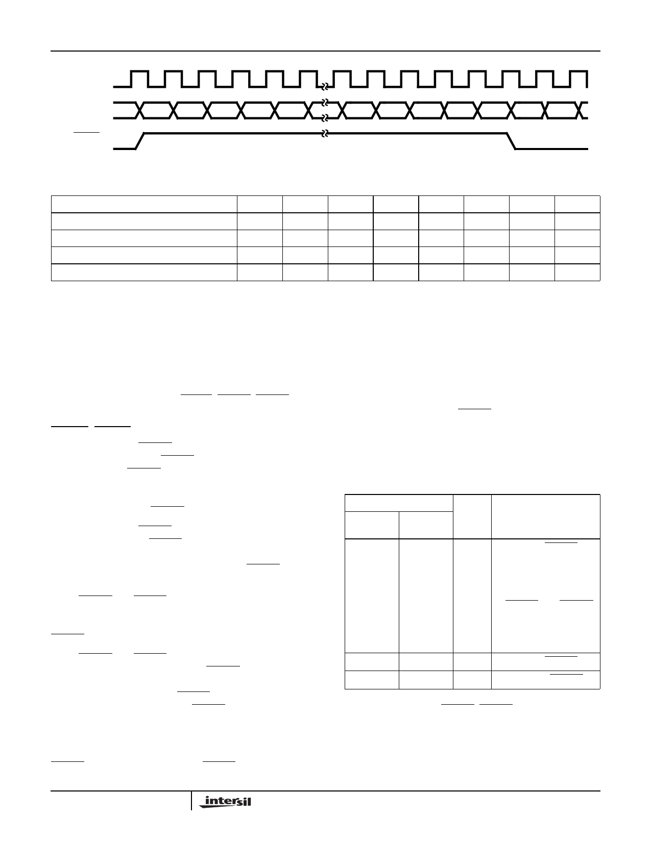
P8-P15 Cb 2 Y 2 Cr 2 Y 3 Cb 4 Y 4
"FF" "00" "00" EAV
"10" "80" "10"
BLANK
(OUTPUT)
FIGURE 3. PIXEL INPUT TIMING - BT.656
TABLE 3. BT.656 EAV AND SAV SEQUENCES
PIXEL INPUT
P15 P14 P13 P12
Preamble Word 1
1111
Preamble Word 2
0000
Preamble Word 3
0000
Status Word
1 FVH
NOTES:
F: 0 = Field 1; 1 = Field 2
V: 0 = Active Line; 1 = Vertical Blanking
H: 0 = Start Active Video; 1 = End Active Video
P3 - P0: Protection bits; Ignored
P11
1
0
0
P3
P10
1
0
0
P2
P9
1
0
0
P1
P8
1
0
0
P0
Video Timing Control
The pixel input data and the output video timing of the
HMP817x are at 50 or 59.94 fields per second interlaced.
The timing is controlled by the BLANK, HSYNC, VSYNC,
FIELD, and CLK2 pins.
HSYNC, VSYNC, and Field Timing
The leading edge of HSYNC indicates the beginning of a
horizontal sync interval. If HSYNC is an output, it is asserted
for about 4.7µs. If HSYNC is an input, it must be active for at
least two CLK2 periods. The width of the analog horizontal
sync tip is determined from the video standard and does not
depend on the width of HSYNC.
The leading edge of VSYNC indicates the beginning of a
vertical sync interval. If VSYNC is an output, it is asserted for
3 scan lines in (MM) NTSC and (M, N) PAL modes or 2.5
scan lines in (B, D, G, H, I, NC) PAL modes. If VSYNC is an
input, it must be asserted for at least two CLK2 periods.
When HSYNC and VSYNC are configured as outputs, their
leading edges will occur simultaneously at the start of an
odd field. At the start of an even field, the leading edge of
VSYNC occurs in the middle of the line.
When HSYNC and VSYNC are configured as inputs, the
HMP817x provides a programmable HSYNC window for
determining FIELD. The window is specified with respect to
the leading or trailing edge of VSYNC. The edge is selected
in the field control register. When HSYNC is found inside the
window, then the encoder sets FIELD to the value specified
in the field control register.
The HMP817x provides programmable timing for the
VSYNC input. At the active edge of VSYNC, the encoder
resets its vertical half-line counter to the value specified by
the field control register. This allows the input and output
syncs to be offset, although the data must still be aligned.
The FIELD signal is always an output and changes state
near each leading edge of VSYNC. The delay between the
syncs and FIELD depends on the encoder’s operating mode
as summarized in Table 4. In modes in which the encoder
uses CLK to gate its inputs and outputs, the FIELD signal
may be delayed 0-12 additional CLK2 periods.
TABLE 4. FIELD OUTPUT TIMING
OPERATING MODE
SYNC I/O BLANK I/O CLK2
DIRECTION DIRECTION DELAY
COMMENTS
Input
Input
148 FIELD lags VSYNC
switching from odd to
even.
FIELD lags the earlier
of VSYNC and HSYNC
when syncs are aligned
when switching from
even to odd.
Input
Output
138 FIELD lags VSYNC.
Output
Don’t Care 32
FIELD leads VSYNC.
Figure 4 illustrates the HSYNC, VSYNC, and FIELD general
timing for (M) NTSC and (M, N) PAL. Figure 5 illustrates the
general timing for (B, D, G, H, I, NC) PAL. In the figures, all
the signals are shown active low (their reset state), and
FIELD is low during odd fields.
5
5 Page 
HMP8170, HMP8171, HMP8172, HMP8173
TABLE 8. BT.656 ANCILLARY DATA FORMAT FOR WIDESCREEN SIGNALLING DATA
PIXEL INPUT
P15 P14 P13 P12 P11 P10
Preamble 1
000000
Preamble 2
111111
Preamble 3
111111
Data ID
ep# ep
1
1
0
0
Data Block Number
ep# ep
0
0
0
0
Data Word Count
ep# ep
0
0
0
0
WSS Data Nibble 3
ep# ep
0
0
0
0
WSS Data Nibble 2
ep# ep
0
0
bit 11
bit 10
WSS Data Nibble 1
ep# ep
0
0 bit 7 bit 6
WSS Data Nibble 0
ep# ep
0
0 bit 3 bit 2
WSS CRC Nibble 1
ep# ep
0
0
0
0
WSS CRC Nibble 0
ep# ep
0
0 bit 3 bit 2
Reserved
ep# ep
0
0
0
0
Reserved
ep# ep
0
0
0
0
CRC
P14#
X
X
X
X
X
NOTES:
The even parity (EP and EP#) bits are ignored.
Line = Data Register Select: 0 = Line 20; 1 = 283.
The WSS CRC data bits are ignored during PAL operation but must be included in the transfer.
X = Don’t Care.
P9
0
1
1
1
0
1
bit 13
bit 9
bit 5
bit 1
bit 5
bit 1
0
0
X
P8
0
1
1
Line
1
0
bit 12
bit 8
bit 4
bit 0
bit 4
bit 0
0
0
X
TABLE 9. WIDESCREEN SIGNALLING MODES
WSS REGISTERS
WSS
ENABLE BITS
OUTPUT LINE(S)
283A, 283B,
CRC283
20A, 20B,
CRC20
00 None
Ignored
Ignored
01 20 (NTSC)
17 (M PAL)
23 (Other PAL)
Ignored
WSS Data
10 283 (NTSC)
280 (M PAL)
336 (Other PAL)
WSS Data
Ignored
11 20, 283 (NTSC)
17, 280 (M PAL)
23, 336 (Other PAL)
WSS Data
WSS Data
NOTE: The CRC registers are always ignored during PAL operation.
WRITE STATUS BIT
283
Always 1
Always 1
20
Always 1
0 = Loaded
1 = Output
0 = Loaded
1 = Output
Always 1
0 = Loaded
1 = Output
0 = Loaded
1 = Output
Teletext
The HMP817x supports ITU-R BT.653 625-line and 525-line
teletext system B and C generation. WST (World System
Teletext) is the same as BT.653 system B. NABTS (North
American Broadcast Teletext Specification) is the same as
BT.653 525-line system C. NABTS is also used to transmit
Intel Intercast information.
During the teletext encoding, the line’s pixel inputs are
ignored. The teletext information includes a 16-bit clock
synchronization code; the HMP817x automatically
generates it.
The teletext output level depends on the video format. For
system B teletext, the output level is 66 IRE for a logic 1 and 0
IRE for a logic 0. All transitions between levels are controlled to
have a raised-cosine shape with a rise or fall time of 200ns. For
system C teletext, the output level is 70 IRE for a logic 1 and 0
IRE for a logic 0. All transitions between levels are controlled to
have a raised-cosine shape with a rise or fall time of 200ns.
The HMP817x generates teletext output on any scan line
that includes teletext data in that line’s BT.656 ancillary data.
The encoder must receive the ancillary data before the SAV
sequence in order to output the teletext data. Table 10 shows
the BT.656 ancillary data format for loading the teletext data
registers.
11
11 Page | ||
| Páginas | Total 30 Páginas | |
| PDF Descargar | [ Datasheet HMP8171CN.PDF ] | |
Hoja de datos destacado
| Número de pieza | Descripción | Fabricantes |
| HMP8171CN | NTSC/PAL Video Encoder | Intersil Corporation |
| Número de pieza | Descripción | Fabricantes |
| SLA6805M | High Voltage 3 phase Motor Driver IC. |
Sanken |
| SDC1742 | 12- and 14-Bit Hybrid Synchro / Resolver-to-Digital Converters. |
Analog Devices |
|
DataSheet.es es una pagina web que funciona como un repositorio de manuales o hoja de datos de muchos de los productos más populares, |
| DataSheet.es | 2020 | Privacy Policy | Contacto | Buscar |
