|
|
|
PDF ADG742BKS Data sheet ( Hoja de datos )
| Número de pieza | ADG742BKS | |
| Descripción | CMOS Low Voltage 2ohm SPST Switches in SC70 Packages | |
| Fabricantes | Analog Devices | |
| Logotipo | ||
Hay una vista previa y un enlace de descarga de ADG742BKS (archivo pdf) en la parte inferior de esta página. Total 8 Páginas | ||
|
No Preview Available !
a
FEATURES
1.8 V to 5.5 V Single Supply
2 ⍀ (Typ) On Resistance
Low On-Resistance Flatness
–3 dB Bandwidth >200 MHz
Rail-to-Rail Operation
6-Lead SC70
Fast Switching Times
tON 18 ns
tOFF 12 ns
Typical Power Consumption (<0.01 W)
TTL/CMOS Compatible
APPLICATIONS
Battery Powered Systems
Communication Systems
Sample Hold Systems
Audio Signal Routing
Video Switching
Mechanical Reed Relay Replacement
CMOS Low Voltage
2 ⍀ SPST Switches in SC70 Packages
ADG741/ADG742
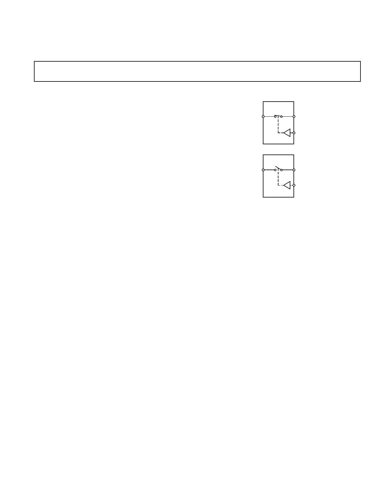
FUNCTIONAL BLOCK DIAGRAMS
ADG741
SD
IN
ADG742
SD
IN
SWITCHES SHOWN FOR
A LOGIC "1" INPUT
GENERAL DESCRIPTION
The ADG741/ADG742 are monolithic CMOS SPST switches.
These switches are designed on an advanced submicron process
that provides low power dissipation yet high switching speed,
low on resistance, low leakage currents and –3 dB bandwidths of
greater than 200 MHz can be achieved.
The ADG741/ADG742 can operate from a single 1.8 V to 5.5 V
supply, making it ideal for use in battery-powered instruments
and with Analog Devices’ new generation of DACs and ADCs.
As can be seen from the Functional Block Diagrams, with a
logic input of “1” the switch of the ADG741 is closed, while
that of the ADG742 is open. Each switch conducts equally well
in both directions when ON.
The ADG741/ADG742 are available in 6-lead SC70 package.
PRODUCT HIGHLIGHTS
1. 1.8 V to 5.5 V Single Supply Operation. The ADG741/
ADG742 offer high performance, including low on resistance
and fast switching times and is fully specified and guaranteed
with 3 V and 5 V supply rails.
2. Very Low RON (3 Ω max at 5 V, 5 Ω max at 3 V). At 1.8 V
operation, RON is typically 40 Ω over the temperature range.
3. On-Resistance Flatness RFLAT(ON) (1 Ω max).
4. –3 dB Bandwidth >200 MHz.
5. Low Power Dissipation. CMOS construction ensures low
power dissipation.
6. Fast tON/tOFF.
7. Tiny 6-Lead SC70 package.
REV. 0
Information furnished by Analog Devices is believed to be accurate and
reliable. However, no responsibility is assumed by Analog Devices for its
use, nor for any infringements of patents or other rights of third parties
which may result from its use. No license is granted by implication or
otherwise under any patent or patent rights of Analog Devices.
One Technology Way, P.O. Box 9106, Norwood, MA 02062-9106, U.S.A.
Tel: 781/329-4700 World Wide Web Site: http://www.analog.com
Fax: 781/326-8703
© Analog Devices, Inc., 2000
1 page 
PIN CONFIGURATIONS
6-Lead Plastic Surface Mount
(SC70)
D 1 ADG741/ 6 VDD
S 2 ADG742 5 NC
GND 3 TOP VIEW 4 IN
(Not to Scale)
NC = NO CONNECT
ADG741/ADG742
TERMINOLOGY
VDD
GND
S
D
IN
RON
RFLAT(ON)
IS (OFF)
ID (OFF)
ID, IS (ON)
VD (VS)
CS (OFF)
CD (OFF)
CD, CS (ON)
tON
tOFF
Off Isolation
Charge
Injection
Bandwidth
On Response
On Loss
Most Positive Power Supply Potential.
Ground (0 V) Reference.
Source Terminal. May be an input or output.
Drain Terminal. May be an input or output.
Logic Control Input.
Ohmic Resistance Between D and S.
Flatness is defined as the difference between
the maximum and minimum value of on
resistance as measured over the specified
analog signal range.
Source Leakage Current with the Switch “OFF.”
Drain Leakage Current with the Switch “OFF.”
Channel Leakage Current with the Switch “ON.”
Analog Voltage on Terminals D, S.
“OFF” Switch Source Capacitance.
“OFF” Switch Drain Capacitance.
“ON” Switch Capacitance.
Delay between applying the digital control
input and the output switching on. See Test
Circuit 4.
Delay between applying the digital control
input and the output switching off.
A measure of Unwanted Signal Coupling
Through an “OFF” Switch.
A measure of the glitch impulse transferred
from the digital input to the analog output
during switching.
The frequency at which the output is attenu-
ated by –3 dBs.
The frequency response of the “ON” switch.
The voltage drop across the “ON” switch seen
on the On Response vs. Frequency plot as how
many dBs the signal is away from 0 dB at very
low frequencies.
REV. 0
–5–
5 Page | ||
| Páginas | Total 8 Páginas | |
| PDF Descargar | [ Datasheet ADG742BKS.PDF ] | |
Hoja de datos destacado
| Número de pieza | Descripción | Fabricantes |
| ADG742BKS | CMOS Low Voltage 2ohm SPST Switches in SC70 Packages | Analog Devices |
| Número de pieza | Descripción | Fabricantes |
| SLA6805M | High Voltage 3 phase Motor Driver IC. |
Sanken |
| SDC1742 | 12- and 14-Bit Hybrid Synchro / Resolver-to-Digital Converters. |
Analog Devices |
|
DataSheet.es es una pagina web que funciona como un repositorio de manuales o hoja de datos de muchos de los productos más populares, |
| DataSheet.es | 2020 | Privacy Policy | Contacto | Buscar |