|
|
|
PDF ADG732 Data sheet ( Hoja de datos )
| Número de pieza | ADG732 | |
| Descripción | 16-/32- Channel/ 3.5 1.8 V to 5.5 V/ 2.5 V/ Analog Multiplexers | |
| Fabricantes | Analog Devices | |
| Logotipo | ||
Hay una vista previa y un enlace de descarga de ADG732 (archivo pdf) en la parte inferior de esta página. Total 13 Páginas | ||
|
No Preview Available !
PRELIMINARY TECHNICAL DATA
= 16-/32- Channel, 3.5 Ω
1.8 V to 5.5 V, ±2.5 V, Analog Multiplexers
Preliminary Technical Data
FEATURES
1.8 V to 5.5 V Single Supply
±2.5 V Dual Supply Operation
3.5 Ω On Resistance
0.5 Ω On Resistance Flatness
Rail to Rail Operation
30ns Switching Times
Single 32 to 1 Channel Multiplexer
Dual/Differential 16 to 1 Channel Multiplexer
TTL/CMOS Compatible Inputs
For Functionally Equivalent devices with Serial Interface
See ADG725/ADG731
APPLICATIONS
Optical Applications
Data Acquisition Systems
Communication Systems
Relay replacement
Audio and Video Switching
Battery Powered Systems
Medical Instrumentation
Automatic Test Equipment
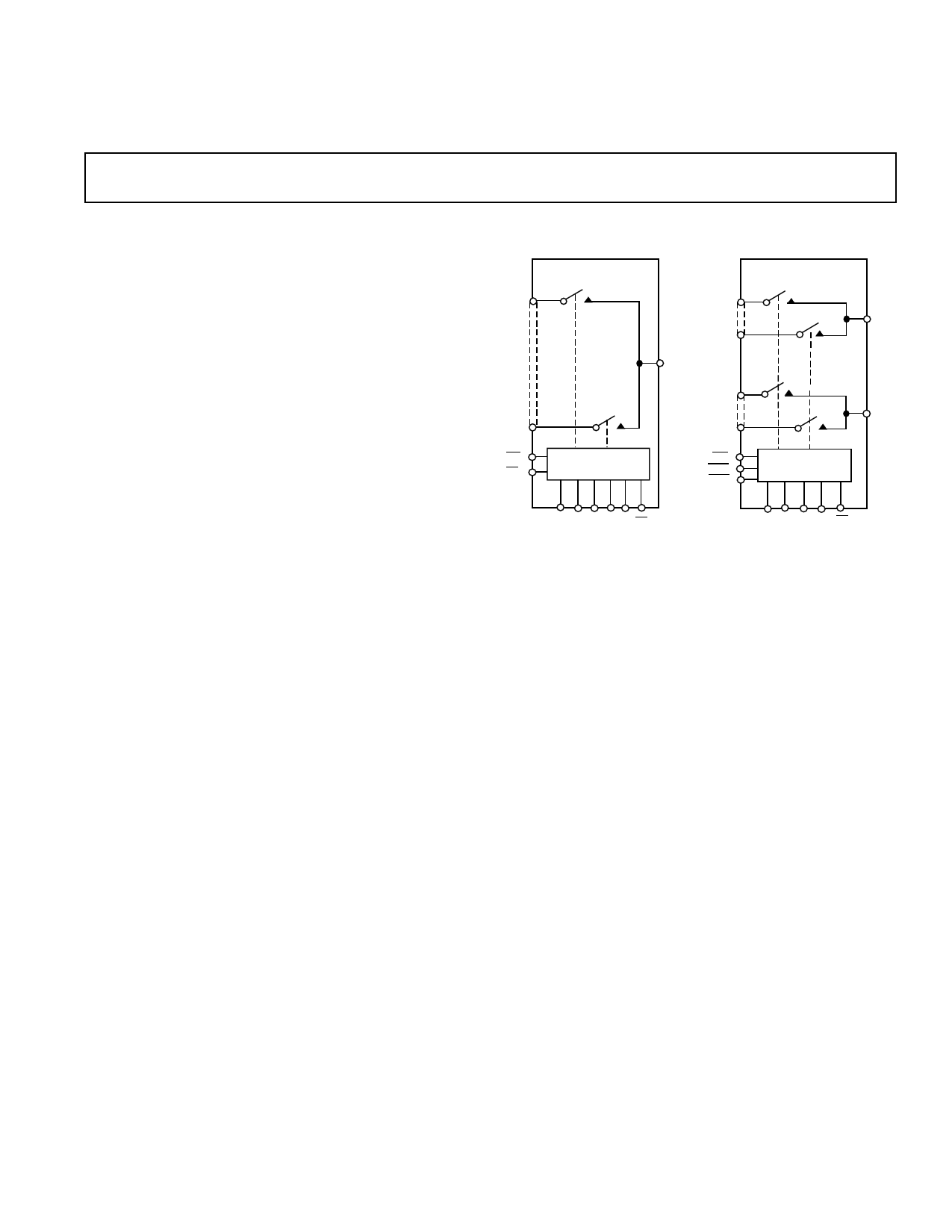
ADG726/ADG732
FUNCTIONAL BLOCK DIAGRAMS
ADG732
S1
S32
WR
CS
1 OF 32
DECODER
S1A
S16A
D
S1B
S16B
WR
CSA
CSB
ADG726
1 OF 16
DECODER
DA
DB
A0 A1 A2 A3 A4 EN
A0 A1 A2 A3 EN
GENERAL DESCRIPTION
The ADG726/ADG732 are monolithic CMOS 32
channel/dual 16 channel analog multiplexers. The
ADG732 switches one of thirty-two inputs (S1-S32) to a
common output, D, as determined by the 5-bit binary
address lines A0, A1, A2, A3 and A4. The ADG726
switches one of sixteen inputs as determined by the four
bit binary address lines, A0, A1, A2 and A3.
On chip latches facilitate microprocessor interfacing. The
ADG726 device may also be configured for differential
operation by tying CSA and CSB together. An EN input
is used to enable or disable the devices. When disabled, all
channels are switched OFF.
These multiplexers are designed on an enhanced submi-
cron process that provides low power dissipation yet gives
high switching speed, very low on resistance and leakage
currents. They operate from single supply of 1.8V to 5.5V
and ±2.5 V dual supply, making them ideally suited to a
variety of applications. On resistance is in the region of a
few Ohms and is closely matched between switches and
very flat over the full signal range. These parts can operate
equally well as either Multiplexers or De-Multiplexers
and have an input signal range which extends to the sup-
plies. In the OFF condition, signal levels up to the
supplies are blocked. All channels exhibit break before
make switching action preventing momentary shorting
when switching channels.
They are available in either 48 lead LFCSP or TQFP
package.
PRODUCT HIGHLIGHTS
1. +1.8 V to +5.5 V Single or ±2.5 V Dual Supply
operation. These parts are specified and guaranteed
with +5 V ±10%, +3 V ±10% single supply and
±2.5 V ±10% dual supply rails.
2. On Resistance of 3.5 Ω.
3. Guaranteed Break-Before-Make Switching Action.
4. 7mm x 7mm 48 lead LF Chip Scale Package (CSP)
or 48 lead TQFP package.
REV. PrD 2001
Information furnished by Analog Devices is believed to be accurate and
reliable. However, no responsibility is assumed by Analog Devices for its
use, nor for any infringements of patents or other rights of third parties
which may result from its use. No license is granted by implication or
otherwise under any patent or patent rights of Analog Devices.
One Technology Way, P.O. Box 9106, Norwood, MA 02062-9106, U.S.A.
Tel: 781/329-4700
World Wide Web Site: http://www.analog.com
Fax: 781/326-8703
Analog Devices, Inc., 2001
1 page 
PRELIMINARY TECHNICAL DATA
ADG726/ADG732
TIMING CHARACTERISTICS1,2, 3
Parameter
Limit at TMIN, TMAX
Units
Conditions/Comments
t1 0
t2 0
t3 20
t4 10
t5 5
t6 2
ns min
ns min
ns min
ns min
ns min
ns min
CS to WR Setup Time
CS to WR Hold Time
WR pulse width
Time between WR cycles
Address, Enable Setup Time
Address, Enable Hold Time
NOTES
1See Figure 1.
2All input signals are specified with tr =tf = 5ns (10% to 90% of VDD) and timed from a voltage level of (VIL + VIH)/2.
3Guaranteed by design and characterisation, not production tested.
Specifications subject to change without notice.
CS
t1 t2
t3 t4
WR
t5 t6
A0, A1, A2, A3, (A4)
EN
Figure 1. Timing Diagram
Figure 1 shows the timing sequence for latching the switch address and enable inputs. The latches are level sensitive;
therefore, while WR is held low, the latches are transparent and the switches respond to the address and enable inputs.
This input data is latched on the rising edge of WR. The ADG726 has two CS inputs. This enables the part to be used
either as a dual 16-1 channel multiplexer or a differential 16 channel multiplexer. If a differential output is required, tie
CSA and CSB together.
REV. PrD
–5–
5 Page 
PRELIMINARY TECHNICAL DATA
ADG726/ADG732
Test Circuits
IDS
V1
S
VS
D
RO N = V1/IDS
Test Circuit 1. On Resistance.
VDD VSS
IS(OFF)
VS
VD
VDD VSS
S1
S2 D
S32
+0.8V
EN
GND
VDD
VSS
VDD
VSS
S1
ID(OFF)
S2 D
A
S3 2
VS
EN
GND
+ 0.8 V
VD
Test Circuit 3. ID (OFF)
VDD VSS
VDD
S1
S3 2
VSS
D
ID (ON)
A
+ 2.4 V
VS
EN
GND
VD
Test Circuit 2. IS (OFF).
Test Circuit 4. ID (ON)
VDD
VSS
3V
VIN 50Ω
VDD
A4
VSS
S1
S2 THRU S31
A0 ADG732* S32
D
EN CS GND WR
VS1
VS32
RL
300 Ω
ADDRESS
DRIVE (VIN )
0V
VOUT
CL
35pF
VS1
VOUT
VS32
50%
90%
* SIMILAR CONNECTION FOR ADG726
tTRANSITION
Test Circuit 5. Switching Time of Multiplexer, tTRANSITION.
50%
90%
tTRANSITION
VIN 50Ω
VDD VSS
VDD
A4
VSS
S1
S2 THRU S31
A0 ADG732*
S32
D
EN CS GND WR
3V
ADDRES S
VS DRIVE (VIN)
0V
RL
300Ω
VOUT
CL
35pF
VS
VOUT
*SIMILAR CONNECTION FOR ADG726
80%
80%
tOPEN
Test Circuit 6. Break Before Make Delay, tOPEN.
REV. PrD
–11–
11 Page | ||
| Páginas | Total 13 Páginas | |
| PDF Descargar | [ Datasheet ADG732.PDF ] | |
Hoja de datos destacado
| Número de pieza | Descripción | Fabricantes |
| ADG731 | 16-/32- Channel/ Serially Controlled 4 1.8 V to 5.5 V/ 2.5 V/ Analog Multiplexers | Analog Devices |
| ADG732 | 16-/32- Channel/ 3.5 1.8 V to 5.5 V/ 2.5 V/ Analog Multiplexers | Analog Devices |
| ADG733 | CMOS/ 2.5 ohm Low Voltage/ Triple/Quad SPDT Switches | Analog Devices |
| ADG734 | CMOS/ 2.5 ohm Low Voltage/ Triple/Quad SPDT Switches | Analog Devices |
| Número de pieza | Descripción | Fabricantes |
| SLA6805M | High Voltage 3 phase Motor Driver IC. |
Sanken |
| SDC1742 | 12- and 14-Bit Hybrid Synchro / Resolver-to-Digital Converters. |
Analog Devices |
|
DataSheet.es es una pagina web que funciona como un repositorio de manuales o hoja de datos de muchos de los productos más populares, |
| DataSheet.es | 2020 | Privacy Policy | Contacto | Buscar |