|
|
|
PDF ADG604 Data sheet ( Hoja de datos )
| Número de pieza | ADG604 | |
| Descripción | 1 pC Charge Injection/ 100 pA Leakage CMOS 5 V/5 V/3 V 4-Channel Multiplexer | |
| Fabricantes | Analog Devices | |
| Logotipo | ||
Hay una vista previa y un enlace de descarga de ADG604 (archivo pdf) en la parte inferior de esta página. Total 12 Páginas | ||
|
No Preview Available !
a 1 pC Charge Injection, 100 pA Leakage
CMOS ؎5 V/5 V/3 V 4-Channel Multiplexer
ADG604
FEATURES
1 pC Charge Injection (Over the Full Signal Range)
؎2.7 V to ؎5.5 V Dual Supply
2.7 V to 5.5 V Single Supply
Automotive Temperature Range: –40؇C to +125؇C
100 pA Max @ 25؇C Leakage Currents
85 ⍀ Typ On Resistance
Rail-to-Rail Operation
Fast Switching Times
Typical Power Consumption (<0.1 W)
TTL/CMOS Compatible Inputs
14-Lead TSSOP Package
APPLICATIONS
Automatic Test Equipment
Data Acquisition Systems
Battery-Powered Instruments
Communication Systems
Sample and Hold Systems
Remote-Powered Equipment
Audio and Video Signal Routing
Relay Replacement
Avionics
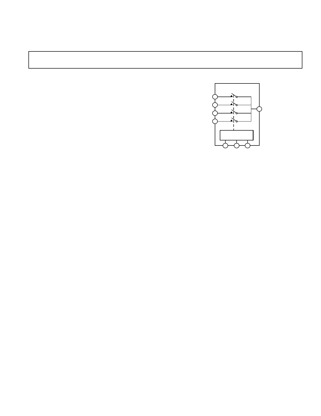
FUNCTIONAL BLOCK DIAGRAM
S1 4
S2 5
S3 11
S4 10
ADG604
6D
1 OF 4
DECODER
1 14 2
A0 A1 EN
GENERAL DESCRIPTION
The ADG604 is a CMOS analog multiplexer, comprising four
single channels. It operates from a dual supply of ± 2.7 V to
± 5.5 V, or from a single supply of 2.7 V to 5.5 V.
The ADG604 switches one of four inputs to a common output,
D, as determined by the 3-bit binary address lines, A0, A1, and
EN. A Logic “0” on the EN pin disables the device.
The ADG604 offers ultralow charge injection of ±1.5 pC over the
entire signal range and leakage currents of 10 pA typical at 25°C.
It offers on resistance of 85 Ω typ, which is matched to within 2 Ω
between channels. The ADG604 also has low power dissipation yet
gives high switching speeds. The ADG604 is available in a 14-lead
TSSOP package.
PRODUCT HIGHLIGHTS
1. Ultralow Charge Injection (Q INJ: ± 1.5 pC Typ over the Full
Signal Range)
2. Leakage Current <0.5 nA max @ 85°C
3. Dual ± 2.7 V to ± 5.5 V or Single 2.7 V to 5.5 V Supply
4. Fully Specified to 125°C
5. Small 14-Lead TSSOP Package
REV. 0
Information furnished by Analog Devices is believed to be accurate and
reliable. However, no responsibility is assumed by Analog Devices for its
use, nor for any infringements of patents or other rights of third parties that
may result from its use. No license is granted by implication or otherwise
under any patent or patent rights of Analog Devices.
One Technology Way, P.O. Box 9106, Norwood, MA 02062-9106, U.S.A.
Tel: 781/329-4700
www.analog.com
Fax: 781/326-8703
© Analog Devices, Inc., 2002
1 page 
ABSOLUTE MAXIMUM RATINGS1
(TA = 25°C unless otherwise noted)
VDD to VSS . . . . . . . . . . . . . . . . . . . . . . . . . . . . . . . . . . . . 13 V
VDD to GND . . . . . . . . . . . . . . . . . . . . . . . . –0.3 V to +6.5 V
VSS to GND . . . . . . . . . . . . . . . . . . . . . . . . . +0.3 V to –6.5 V
Analog Inputs2 . . . . . . . . . . . . . . . . VSS –0.3 V to VDD + 0.3 V
Digital Inputs2 . . . . . . . . . . . . . . . . . –0.3 V to VDD + 0.3 V or
. . . . . . . . . . . . . . . . . . . . . . 30 mA, Whichever Occurs First
Peak Current, S or D . . . . . . . . . . . . . . . . . . . . . . . . . . 20 mA
(Pulsed at 1 ms, 10% Duty Cycle Max)
Continuous Current, S or D . . . . . . . . . . . . . . . . . . . . 10 mA
Operating Temperature Range
Automotive (Y Version) . . . . . . . . . . . . . . –40°C to +125°C
Storage Temperature Range . . . . . . . . . . . . –65°C to +150°C
ADG604
Junction Temperature . . . . . . . . . . . . . . . . . . . . . . . . . 150°C
TSSOP Package
JA Thermal Impedance . . . . . . . . . . . . . . . . . . . . 150°C/W
JC Thermal Impedance . . . . . . . . . . . . . . . . . . . . . 27°C/W
Lead Temperature, Soldering (10 seconds) . . . . . . . . . 300°C
IR Reflow, Peak Temperature . . . . . . . . . . . . . . . . . 220°C
NOTES
1Stresses above those listed under Absolute Maximum Ratings may cause perma-
nent damage to the device. This is a stress rating only; functional operation of the
device at these or any other conditions above those listed in the operational
sections of this specification is not implied. Exposure to absolute maximum rating
conditions for extended periods may affect device reliability. Only one absolute
maximum rating may be applied at any one time.
2Overvoltages at EN, A0, A1, S, or D will be clamped by internal diodes. Current
should be limited to the maximum ratings given.
Model Option
ADG604YRU
ORDERING GUIDE
Temperature Range
–40°C to +125°C
Package Description
Thin Shrink Small Outline (TSSOP)
Package
RU-14
PIN CONFIGURATION
A0 1
14 A1
EN 2
13 GND
VSS 3 ADG604 12 VDD
TOP VIEW
S1 4 (Not To Scale) 11 S3
S2 5
10 S4
D6
9 NC
NC 7
8 NC
NC = NO CONNECT
Table I. Truth Table
A1 A0 EN ON Switch
X X 0 None
00 11
01 12
10 13
11 14
CAUTION
ESD (electrostatic discharge) sensitive device. Electrostatic charges as high as 4000 V readily
accumulate on the human body and test equipment and can discharge without detection. Although
the ADG604 features proprietary ESD protection circuitry, permanent damage may occur on
devices subjected to high-energy electrostatic discharges. Therefore, proper ESD precautions are
recommended to avoid performance degradation or loss of functionality.
WARNING!
ESD SENSITIVE DEVICE
REV. 0
–5–
5 Page 
OUTLINE DIMENSIONS
Dimensions shown in inches and (mm).
14-Lead TSSOP Package
(RU-14)
0.201 (5.10)
0.193 (4.90)
14
1
PIN 1
0.006 (0.15)
0.002 (0.05)
8
0.177 (4.50)
0.169 (4.30)
0.256 (6.50)
0.246 (6.25)
7
0.0433 (1.10)
MAX
SEATING
PLANE
0.0256
(0.65)
BSC
0.0118 (0.30)
0.0075 (0.19)
8؇
0.0079 (0.20) 0؇
0.0035 (0.090)
0.028 (0.70)
0.020 (0.50)
ADG604
REV. 0
–11–
11 Page | ||
| Páginas | Total 12 Páginas | |
| PDF Descargar | [ Datasheet ADG604.PDF ] | |
Hoja de datos destacado
| Número de pieza | Descripción | Fabricantes |
| ADG601 | SPST Switches | Analog Devices |
| ADG602 | SPST Switches | Analog Devices |
| ADG604 | 1 pC Charge Injection/ 100 pA Leakage CMOS 5 V/5 V/3 V 4-Channel Multiplexer | Analog Devices |
| ADG608 | 3 V/5 V/ 4/8 Channel High Performance Analog Multiplexers | Analog Devices |
| Número de pieza | Descripción | Fabricantes |
| SLA6805M | High Voltage 3 phase Motor Driver IC. |
Sanken |
| SDC1742 | 12- and 14-Bit Hybrid Synchro / Resolver-to-Digital Converters. |
Analog Devices |
|
DataSheet.es es una pagina web que funciona como un repositorio de manuales o hoja de datos de muchos de los productos más populares, |
| DataSheet.es | 2020 | Privacy Policy | Contacto | Buscar |