|
|
|
PDF ADC701 Data sheet ( Hoja de datos )
| Número de pieza | ADC701 | |
| Descripción | 16-Bit 512kHz SAMPLING A/D CONVERTER SYSTEM | |
| Fabricantes | Burr-Brown Corporation | |
| Logotipo | ||
Hay una vista previa y un enlace de descarga de ADC701 (archivo pdf) en la parte inferior de esta página. Total 15 Páginas | ||
|
No Preview Available !
® ADC701
SHC702
16-Bit 512kHz
SAMPLING A/D CONVERTER SYSTEM
FEATURES
q CONVERSION RATE: to 512kHz Over
Temp
q NO MISSING CODES AT 16 BITS
q SPURIOUS-FREE DYNAMIC RANGE:
107dB
q LOW NONLINEARITY: ±0.0015%
q SELECTABLE INPUT RANGES: ±5V,
±10V, 0 to +10V, 0 to +5V, –10V to 0
q LOW POWER DISSIPATION: 2.8W Typical
Including Sample/Hold
q METAL AND CERAMIC DIP PACKAGES
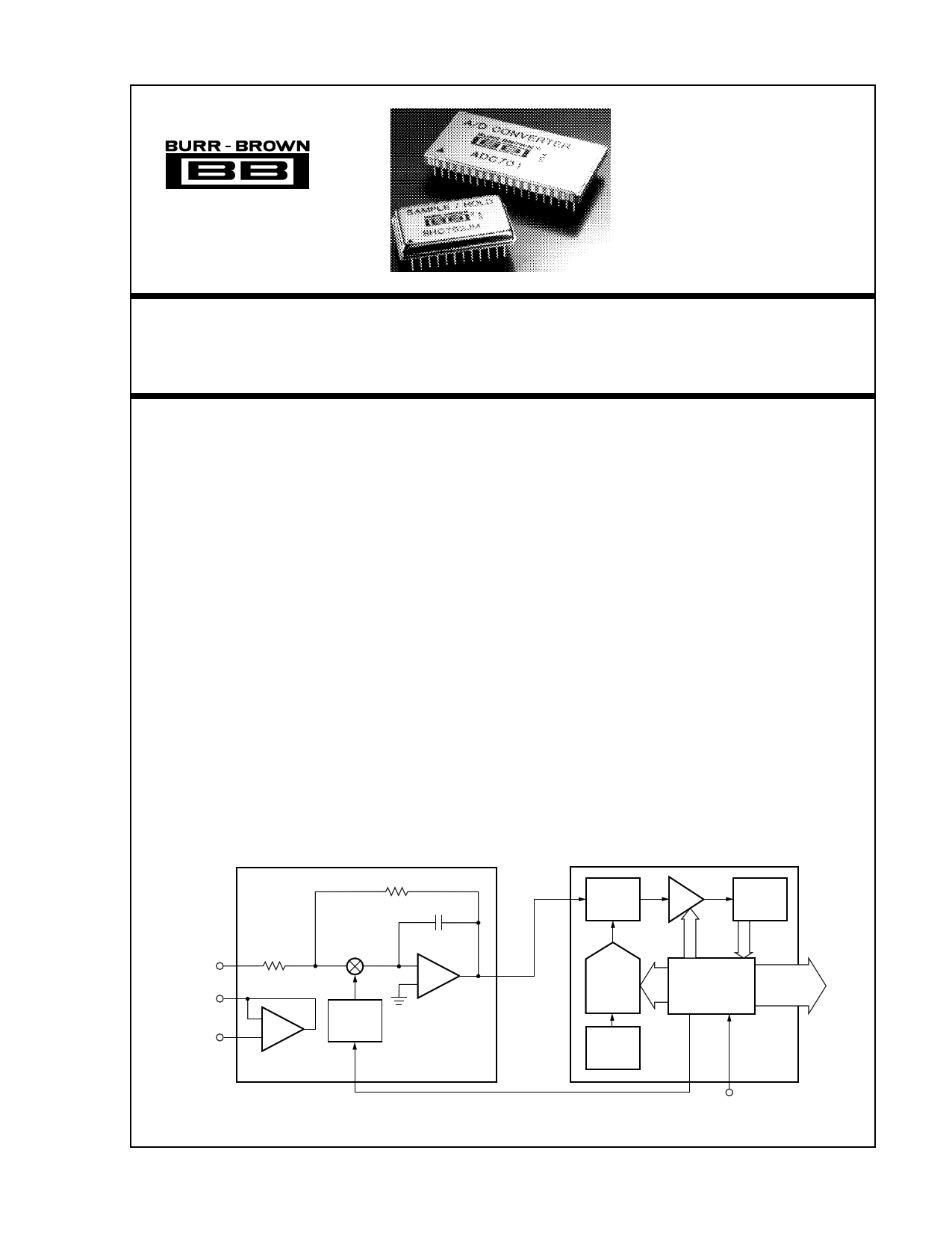
DESCRIPTION
The ADC701 is a very high speed 16-bit analog-to-
digital converter based on a three-step subranging
architecture. Outstanding dynamic performance is
achieved with the SHC702 companion sample/hold
amplifier. Both devices use hybrid construction for
applications where reliability, small size, and low
power consumption are especially important.
1k Ω
APPLICATIONS
q MEDICAL IMAGING
q SONAR
q PROFESSIONAL AUDIO RECORDING
q AUTOMATIC TEST EQUIPMENT
q HIGH PERFORMANCE FFT SPECTRUM
ANALYSIS
q ULTRASOUND SIGNAL PROCESSING
q HIGH SPEED DATA ACQUISITION
q REPLACES DISCRETE MODULAR ADCs
Excellent linearity and stability are assured through
use of a new ultra-precise monolithic D/A converter
and a low-drift reference circuit. Custom monolithic
op amps provide very high bandwidth and low noise
in all sections of the analog signal path. Logic is
CMOS/TTL compatible and is designed for maxi-
mum flexibility.
Input
Scaling
Network
PGA
Flash
Encoder
Analog
Input
Buffer
Output
Buffer
Input
1k Ω
–
+
Switch
Drive
–
+ DAC
SHC702
Sample/Hold
Command
10V
Ref
Timing and
Control Logic
Data
Output
ADC701
Convert Command
InternationalAirportIndustrialPark • MailingAddress:POBox11400,Tucson,AZ85734 • StreetAddress:6730S.TucsonBlvd.,Tucson,AZ 85706 • Tel:(520)746-1111 • Twx:910-952-1111
Internet:http://www.burr-brown.com/ • FAXLine:(800)548-6133(US/CanadaOnly) • Cable:BBRCORP • Telex:066-6491 • FAX:(520)889-1510 • ImmediateProductInfo:(800)548-6132
© 1988 Burr-Brown Corporation
PDS-877D
Printed in U.S.A. May, 1997
1 page 
ADC701 OUTPUT CODING
INPUT LEVEL
(Exact Center of Code)
Underrange
–FS
–FS + 1LSB
–3/4FS
–1/2FS
–1/4FS
–1LSB
Mid-Scale
+1LSB
+1/4FS
+1/2FS
+3/4FS
+FS –2LSB
+FS – 1LSB
Overrange
NOMINAL INPUT VOLTAGE TO ADC701
(Multiply by –1 for SHC702 Input Voltage)
0–10V RANGE
(1LSB ≈153µV)
±10V RANGE
(1LSB ≈05µV
±5V RANGE
(1LSB ≈153µV)
< –76µV
0V
+153µV
< –10.000153V
–10V
–9.999695V
< –5.000076V
–5V
–4.999847V
+1.25V
+2.5V
+3.75V
–7.5V
–5V
–2.5V
–3.75V
–2.5V
–1.25V
+4.999847V
+5V
+5.000153V
–305µV
0V
+305µV
–153µV
0V
+153µV
+6.25V
+7.5V
+8.75V
+2.5V
+5V
+7.5V
+1.25V
+2.5V
+3.75V
+9.999695V
+9.999847V
> +9.999924V
+9.99939V
+9.999695V
> +9.999847V
+4.999695V
+4.999847V
> +4.999924V
OUTPUT CODE
(1 = Logic High)
MSB
LSB
0000 0000 0000 0000
0000 0000 0000 0000
0000 0000 0000 0001
0010 0000 0000 0000
0100 0000 0000 0000
0110 0000 0000 0000
0111 1111 1111 1111
1000 0000 0000 0000
1000 0000 0000 0001
1010 0000 0000 0000
1100 0000 0000 0000
1110 0000 0000 0000
1111 1111 1111 1110
1111 1111 1111 1111
1111 1111 1111 1111
CLIP
DETECT
1
0
0
0
0
0
0
0
0
0
0
0
0
0
1
SHC702 PIN ASSIGNMENTS
PIN NO.
1
2
3
4
5
6
7
8
9
10
11
12
DESCRIPTION
Sample/Hold Output
NC(3)
NC
NC
NC
NC
NC
NC
+VDD1 (+5V) Analog
Common (Digital)
Hold Input(1)
Hold Input(1)
PIN NO.
24
23
22
21
20
19
18
17
16
15
14
13
DESCRIPTION
+VCC (+15V) Analog
Common (Power)
–VCC (–15V) Analog
Common (Analog)
NC
NC
NC
Buffer Amp Input(2)
NC
Common (Signal)
Buffer Amp Output
Analog Input
NOTES: (1) Hold mode is activated only when pin 12 is low and pin 11 is high.
For normal use with ADC701, pin 12 is grounded and pin 11 is connected to
ADC701 Sample/Hold control (ADC701 pin 15). (2) If the buffer amp is not used,
pin 17 should be grounded. (3) NC = No Internal Connection.
PACKAGING INFORMATION
PRODUCT
PACKAGE
PACKAGE DRAWING
NUMBER(1)
SHC702JM
24-Pin
037
NOTE: (1) For detailed drawing and dimension table, please see end of data
sheet, or Appendix C of Burr-Brown IC Data Book.
SHC702 ORDERING INFORMATION
Basic Model Number
Performance Grade Code
J: 0°C to +70°C Ambient Temperature
Package Code
M: Metal
SHC702 J M
SHC702 ABSOLUTE MAXIMUM RATINGS
±Vcc .................................................................................................... ±18V
+VDD1 ................................................................................................... +7V
Analog and Buffer Inputs ................................................................... ±VCC
Outputs .......................................................... Indefinite Short to Common
Logic Inputs ........................................................... –0.5V to (+VDD1 + 0.3V)
Case Temperature ........................................................................ +150°C
Junction Temperature ................................................................... +165°C
Storage Temperature ...................................................... –65°C to +165°C
Power Dissipation .............................................................................. 1.5W
Stresses above these ratings may permanently damage the device.
The information provided herein is believed to be reliable; however, BURR-BROWN assumes no responsibility for inaccuracies or omissions. BURR-BROWN assumes
no responsibility for the use of this information, and all use of such information shall be entirely at the user's own risk. Prices and specifications are subject to change
without notice. No patent rights or licenses to any of the circuits described herein are implied or granted to any third party. BURR-BROWN does not authorize or warrant
any BURR-BROWN product for use in life support devices and/or systems.
®
5 ADC701/SHC702
5 Page 
ADC701 Digital I/O
Refer to the timing diagram, Figure 4. The conversion
process is initiated by a rising edge on the Convert Com-
mand input. This will immediately bring the sample/hold
command output to a logic high state (Hold mode).
After the ADC701 conversion is completed (approximately
1.5µs after the convert command edge), the Sample/Hold
Command falls to a low state, enabling the sample/hold to
begin acquisition of the next input sample. However, the
ADC701 internal clock continues to run so that the output
data may be processed.
There are two methods of reading data from the ADC:
1. Strobed Output—This will usually be the easiest and
fastest method. The data are presented sequentially as
high and low bytes of the total 16-bit word. The sequence
High-Low or Low-High is controlled by the state of the
High/Low Byte Select input. The first byte is valid on the
rising edge of the Data Strobe output; the second byte is
valid on the falling edge.
2. Polled output—With this method, data strobes will occur
as described above, but they are ignored by the user.
Instead, the user waits until the Data Strobe output falls,
and then manually selects high and low output data by
means of the High/Low Byte Select input. This polling
procedure may be carried out during the subsequent ADC
conversion cycle, but two precautions must be observed:
First, the user should avoid switching the High/Low Byte
Select immediately before or after the next convert com-
mand. This will prevent digital switching noise from
coupling into the system at the instant of analog sam-
pling. Second, the polling sequence must be completed
before the ADC begins to strobe out data from the
subsequent conversion.
OPTIONS FOR STROBED OUTPUT
There are several ways in practice to implement the logic
interface. Figure 3 shows the simplest configurations. In
order to convert the ADC701’s byte-sequential data into 16-
bit parallel form, the minimum requirement is for one single
octal flip-flop, such as a 74HC574 or equivalent. This will
latch the first byte on the rising edge of the ADC701 Data
Strobe. Then the second byte becomes valid, and all 16 bits
may be strobed to the outside system on the falling edge of
the Data Strobe.
For better noise isolation of the ADC701 from the digital
system, or if full three-state capability is required for the 16
output lines, a second octal flip-flop can be added as shown
in the dashed lines of Figure 3. This will also require an
inverter to convert the falling Data Strobe edge into a rising
clock edge for the second flip-flop IC.
If it is desirable to have all 16 output lines change simulta-
neously (for example when driving a D/A converter), then a
third octal flip-flop (not shown in Figure 3) may be added to
re-latch the output of the first byte. By driving that device’s
clock also from the inverted Data Strobe, fully synchronous
switching of the 16 output bits will be achieved.
USING THE CLIP DETECT OUTPUT
The ADC701 provides a built-in Clip Detect signal on pin 9
which indicates an ADC overrange or underrange condition.
The Clip Detect signal is only valid when the High Byte
becomes valid as shown in Figure 4. Therefore, the simplest
way to latch the Clip Detect signal is to provide an extra flip-
flop which is clocked on the same strobe edge as the High
Byte flip-flop. Such a setup is illustrated in Figure 3. The
Clip Detect signal remains at logic 0 under normal condi-
tions, and indicates a clip condition by rising to a logic 1.
Start Conversion
N
ADC701
Convert Command
(CC)
50ns min
CC to Hold delay 18ns typ
Hold Command
to SHC702
Hold Mode
1.45µs typ
Data Outputs for
Pin 13 = Low
Low Byte,(4)
Data N – 1
Data Outputs for
Pin 13 = High
High Byte,(3)
Data N – 1
Data Strobe Output
1.55µs typ
50ns min
Start Conversion
N+1
Sample Mode
High Byte,(3)
Data N
Low Byte,(4)
Data N
Low Byte,(4)
Data N
High Byte,(3)
Data N
(2)
(1) (1)
110ns
typ
NOTES: (1) Setup Time 28ns min, 37ns typ. (2) Hold Time 30ns min, 73ns typ. (3) High Byte refers to ADC bits 1 - 8, the most significant 8 bits.
Also, the Clip Detect signal on pin 9 is valid simultaneously with High Byte. (4) Low Byte refers to ADC bits 9 - 16, the least significant bits.
FIGURE 4. ADC701 Interface Timing Diagram.
11 ADC701/SHC702
®
11 Page | ||
| Páginas | Total 15 Páginas | |
| PDF Descargar | [ Datasheet ADC701.PDF ] | |
Hoja de datos destacado
| Número de pieza | Descripción | Fabricantes |
| ADC700 | 16-Bit Resolution With Microprocessor Interface A/D CONVERTER | Burr-Brown Corporation |
| ADC700AH | 16-Bit Resolution With Microprocessor Interface A/D CONVERTER | Burr-Brown Corporation |
| ADC700BH | 16-Bit Resolution With Microprocessor Interface A/D CONVERTER | Burr-Brown Corporation |
| ADC700JH | 16-Bit Resolution With Microprocessor Interface A/D CONVERTER | Burr-Brown Corporation |
| Número de pieza | Descripción | Fabricantes |
| SLA6805M | High Voltage 3 phase Motor Driver IC. |
Sanken |
| SDC1742 | 12- and 14-Bit Hybrid Synchro / Resolver-to-Digital Converters. |
Analog Devices |
|
DataSheet.es es una pagina web que funciona como un repositorio de manuales o hoja de datos de muchos de los productos más populares, |
| DataSheet.es | 2020 | Privacy Policy | Contacto | Buscar |