|
|
PDF ADC12H030 Data sheet ( Hoja de datos )
| Número de pieza | ADC12H030 | |
| Descripción | Self-Calibrating 12-Bit Plus Sign Serial I/O A/D Converters with MUX and Sample/Hold | |
| Fabricantes | National Semiconductor | |
| Logotipo | ||
Hay una vista previa y un enlace de descarga de ADC12H030 (archivo pdf) en la parte inferior de esta página. Total 30 Páginas | ||
|
No Preview Available !
July 1999
ADC12H030/ADC12H032/ADC12H034/ADC12H038,
ADC12030/ADC12032/ADC12034/ADC12038
Self-Calibrating 12-Bit Plus Sign Serial I/O A/D
Converters with MUX and Sample/Hold
General Description
The ADC12030, and ADC12H030 families are 12-bit plus
sign successive approximation A/D converters with serial I/O
and configurable input multiplexers. The ADC12032/
ADC12H032, ADC12034/ADC12H034 and ADC12038/
ADC12H038 have 2, 4 and 8 channel multiplexers, respec-
tively. The differential multiplexer outputs and A/D inputs are
available on the MUXOUT1, MUXOUT2, A/DIN1 and A/DIN2
pins. The ADC12030/ADC12H030 has a two channel multi-
plexer with the multiplexer outputs and A/D inputs internally
connected. The ADC12030 family is tested with a 5 MHz
clock, while the ADC12H030 family is tested with an 8 MHz
clock. On request, these A/Ds go through a self calibration
process that adjusts linearity, zero and full-scale errors to
less than ±1 LSB each.
The analog inputs can be configured to operate in various
combinations of single-ended, differential, or
pseudo-differential modes. A fully differential unipolar analog
input range (0V to +5V) can be accommodated with a single
+5V supply. In the differential modes, valid outputs are ob-
tained even when the negative inputs are greater than the
positive because of the 12-bit plus sign output data format.
The serial I/O is configured to comply with the
NSC MICROWIRE™. For voltage references see the
LM4040 or LM4041.
Features
n Serial I/O (MICROWIRE Compatible)
n 2, 4, or 8 channel differential or single-ended multiplexer
n Analog input sample/hold function
n Power down mode
n Variable resolution and conversion rate
n Programmable acquisition time
n Variable digital output word length and format
n No zero or full scale adjustment required
n Fully tested and guaranteed with a 4.096V reference
n 0V to 5V analog input range with single 5V power
supply
n No Missing Codes over temperature
Key Specifications
n Resolution
n 12-bit plus sign conversion time
— ADC12H030 family
— ADC12030 family
n 12-bit plus sign throughput time
— ADC12H030 family
— ADC12030 family
n Integral linearity error
n Single supply
n Power dissipation
— Power down
12-bit plus sign
5.5 µs (max)
8.8 µs (max)
8.6 µs (max)
14 µs (max)
±1 LSB (max)
5V ±10%
33 mW (max)
100 µW (typ)
Applications
n Medical instruments
n Process control systems
n Test equipment
TRI-STATE® is a registered trademark of National Semiconductor Corporation.
COPS™ microcontrollers, HPC™ and MICROWIRE™ are trademarks of National Semiconductor Corporation.
© 1999 National Semiconductor Corporation DS011354
www.national.com
1 page 
Absolute Maximum Ratings (Notes 1, 2)
If Military/Aerospace specified devices are required,
please contact the National Semiconductor Sales Office/
Distributors for availability and specifications.
Positive Supply Voltage
(V+ = VA+ = VD+)
Voltage at Inputs and Outputs
except CH0–CH7 and COM
Voltage at Analog Inputs
CH0–CH7 and COM
|VA+ − VD+|
Input Current at Any Pin (Note 3)
Package Input Current (Note 3)
Package Dissipation at
TA = 25˚C (Note 4)
ESD Susceptability (Note 5)
Human Body Model
Soldering Information
N Packages (10 seconds)
SO Package (Note 6):
Vapor Phase (60 seconds)
Infrared (15 seconds)
Storage Temperature
6.5V
−0.3V to V+ +0.3V
GND −5V to V+ +5V
300 mV
±30 mA
±120 mA
500 mW
1500V
260˚C
215˚C
220˚C
−65˚C to +150˚C
Operating Ratings (Notes 1, 2)
Operating Temperature Range
ADC12030CIWM,
ADC12H030CIWM,
ADC12032CIWM,
ADC12H032CIWM,
ADC12034CIN, ADC12034CIWM,
ADC12H034CIN,
ADC12H034CIWM,
ADC12038CIWM,
ADC12H038CIWM
Supply Voltage (V+ = VA+ = VD+)
|VA+ − VD+|
VREF+
VREF−
VREF (VREF+ − VREF−)
VREF Common Mode Voltage Range
TMIN ≤ TA ≤ TMAX
−40˚C ≤ TA ≤ +85˚C
+4.5V to +5.5V
≤ 100 mV
0V to VA+
0V to VREF+
1V to VA+
A/DIN1, A/DIN2, MUXOUT1
and MUXOUT2 Voltage Range
A/D IN Common Mode
Voltage Range
0.1 VA+ to 0.6 VA+
0V to VA+
0V to VA+
Converter Electrical Characteristics
sATihDoenCf1mo2lol0od3we0i,n, fgACKDspC=e1cf2Sif0Kic3a=2t,io8AnMDs CHa1zp2pf0oly3r 4ftohraenVAd+DA=CD1VC2A1H+200=330V8,D,A+RDS=C=1+252H.500Ω3V,2Ds,CoA,uDVrcRCeE1Fi2m+Hp=0e3d+4a4na.0cn9ed6fAoVrDDVCCR1, E2VFHR+0Ea3F−n8d,=fVC0KREV=FD−fCS≤,K12=25-Ω5bi,Mt f+uHlslzyig-fdonirffctehorenevnetira-l
input with fixed 2.048V common-mode voltage,
for TA = TJ = TMIN to TMAX; all other limits TA
and
= TJ
1=0(2tC5K˚C) .ac(Nquoitseistio7n,
time
8, 9)
unless
otherwise
specified.
Boldface
limits
apply
Symbol
Parameter
Conditions
Typical
(Note 10)
Limits
(Note 11)
Units
(Limits)
STATIC CONVERTER CHARACTERISTICS
+ILE
−ILE
DNL
TUE
Resolution with No
Missing Codes
Positive Integral Linearity Error
Negative Integral Linearity Error
Differential Non-Linearity
Positive Full-Scale Error
Negative Full-Scale Error
Offset Error
DC Common Mode Error
Total Unadjusted Error
After Auto-Cal (Notes 12, 18)
After Auto-Cal (Notes 12, 18)
After Auto-Cal
After Auto-Cal (Notes 12, 18)
After Auto-Cal (Notes 12, 18)
After Auto-Cal (Notes 5, 18)
VIN(+) = VIN (−) = 2.048V
After Auto-Cal (Note 15)
After Auto-Cal
±1/2
±1/2
±1/2
±1/2
±1/2
±2
±1
12 + sign Bits (min)
±1
±1
±1
±3.0
±3.0
±2
LSB (max)
LSB (max)
LSB (max)
LSB (max)
LSB (max)
LSB (max)
±3.5
LSB (max)
LSB
(Notes 12, 13, 14)
+INL
−INL
DNL
Resolution with No
Missing Codes
Positive Integral Linearity Error
Negative Integral Linearity Error
Differential Non-Linearity
Positive Full-Scale Error
Negative Full-Scale Error
8-bit + sign mode
8-bit + sign mode (Note 12)
8-bit + sign mode (Note 12)
8-bit + sign mode
8-bit + sign mode (Note 12)
8-bit + sign mode (Note 12)
8 + sign Bits (min)
±1/2
±1/2
±3/4
±1/2
±1/2
LSB (max)
LSB (max)
LSB (max)
LSB (max)
LSB (max)
5 www.national.com
5 Page 
AC Electrical Characteristics (Continued)
Note 9: With the test condition for VREF (VREF+ − VREF−) given as +4.096V, the 12-bit LSB is 1.0 mV and the 8-bit LSB is 16.0 mV.
Note 10: Typicals are at TJ = TA = 25˚C and represent most likely parametric norm.
Note 11: Tested limits are guaranteed to National’s AOQL (Average Outgoing Quality Level).
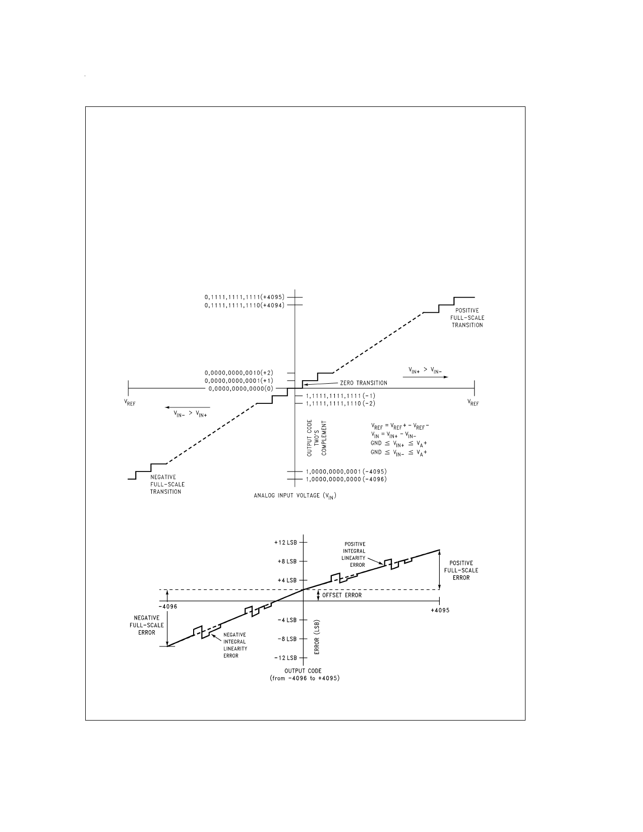
Note 12: Positive integral linearity error is defined as the deviation of the analog value, expressed in LSBs, from the straight line that passes through positive
full-scale and zero. For negative integral linearity error, the straight line passes through negative full-scale and zero (see Figures 2, 3).
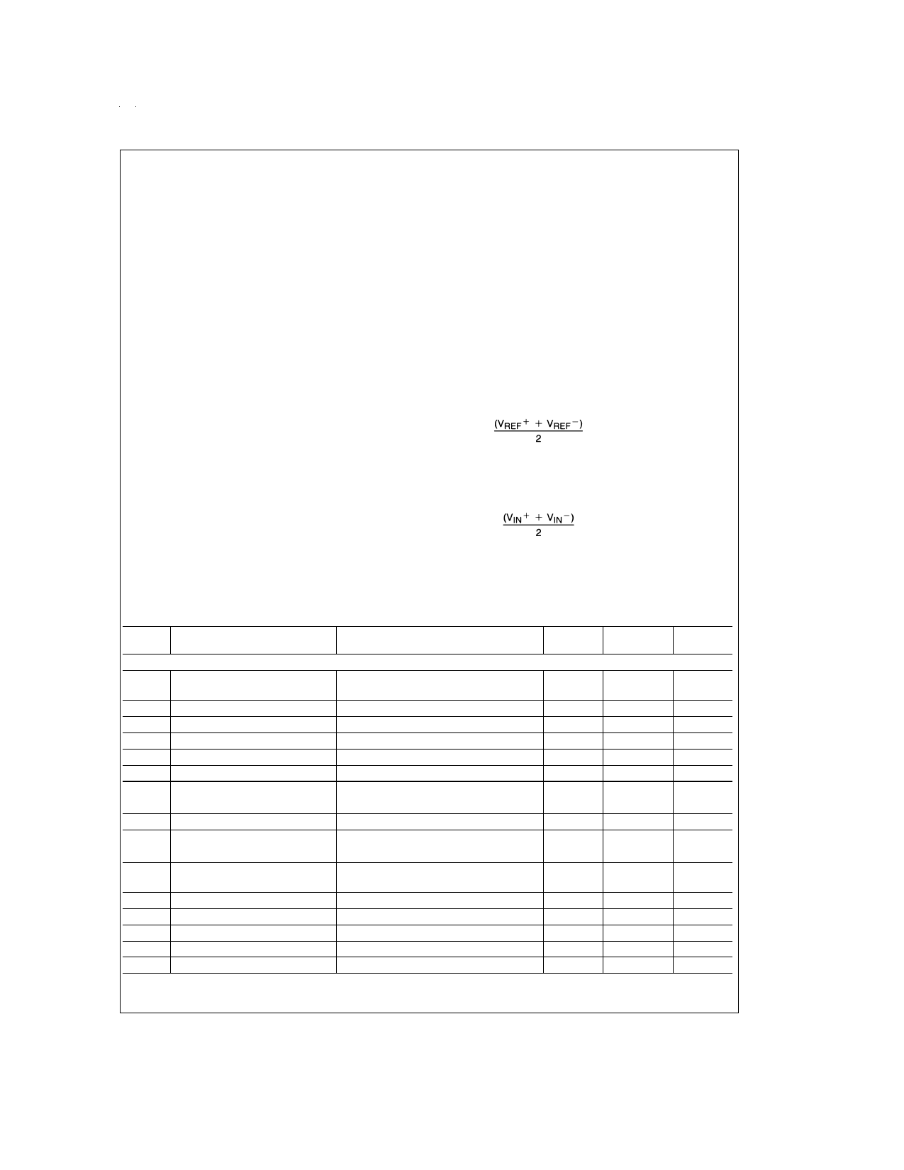
Note 13: Zero error is a measure of the deviation from the mid-scale voltage (a code of zero), expressed in LSB. It is the worst-case value of the code transitions
between 1 to 0 and 0 to +1 (see Figure 4).
Note 14: Total unadjusted error includes offset, full-scale, linearity and multiplexer errors.
Note 15: The DC common-mode error is measured in the differential multiplexer mode with the assigned positive and negative input channels shorted together.
Note 16: Channel leakage current is measured after the channel selection.
Note 17: Timing specifications are tested at the TTL logic levels, VIL = 0.4V for a falling edge and VIH = 2.4V for a rising edge. TRI-STATE output voltage is forced
to 1.4V.
Note 18: The ADC12030 family’s self-calibration technique ensures linearity and offset errors as specified, but noise inherent in the self-calibration process will re-
sult in a maximum repeatability uncertainty of 0.2 LSB.
Note 19: If SCLK and CCLK are driven from the same clock source, then tA is 6, 10, 18 or 34 clock periods minimum and maximum.
Note 20: The “12-Bit Conversion of Offset” and “12-Bit Conversion of Full-Scale” modes are intended to test the functionality of the device. Therefore, the output
data from these modes are not an indication of the accuracy of a conversion result.
FIGURE 1. Transfer Characteristic
DS011354-10
DS011354-11
FIGURE 2. Simplified Error Curve vs Output Code without Auto-Calibration or Auto-Zero Cycles
11 www.national.com
11 Page | ||
| Páginas | Total 30 Páginas | |
| PDF Descargar | [ Datasheet ADC12H030.PDF ] | |
Hoja de datos destacado
| Número de pieza | Descripción | Fabricantes |
| ADC12H030 | Self-Calibrating 12-Bit Plus Sign Serial I/O A/D Converters with MUX and Sample/Hold | National Semiconductor |
| ADC12H032 | Self-Calibrating 12-Bit Plus Sign Serial I/O A/D Converters with MUX and Sample/Hold | National Semiconductor |
| ADC12H034 | Self-Calibrating 12-Bit Plus Sign Serial I/O A/D Converters with MUX and Sample/Hold | National Semiconductor |
| ADC12H038 | Self-Calibrating 12-Bit Plus Sign Serial I/O A/D Converters with MUX and Sample/Hold | National Semiconductor |
| Número de pieza | Descripción | Fabricantes |
| SLA6805M | High Voltage 3 phase Motor Driver IC. |
Sanken |
| SDC1742 | 12- and 14-Bit Hybrid Synchro / Resolver-to-Digital Converters. |
Analog Devices |
|
DataSheet.es es una pagina web que funciona como un repositorio de manuales o hoja de datos de muchos de los productos más populares, |
| DataSheet.es | 2020 | Privacy Policy | Contacto | Buscar |
