|
|
|
PDF ADC12048EVAL Data sheet ( Hoja de datos )
| Número de pieza | ADC12048EVAL | |
| Descripción | 12-Bit Plus Sign 216 kHz 8-Channel Sampling Analog-to-Digital Converter | |
| Fabricantes | National Semiconductor | |
| Logotipo | ||
Hay una vista previa y un enlace de descarga de ADC12048EVAL (archivo pdf) en la parte inferior de esta página. Total 30 Páginas | ||
|
No Preview Available !
April 2000
ADC12048
12-Bit Plus Sign 216 kHz 8-Channel Sampling
Analog-to-Digital Converter
General Description
Operating from a single 5V power supply, the ADC12048 is a
12 bit + sign, parallel I/O, self-calibrating, sampling
analog-to-digital converter (ADC) with an eight input fully dif-
ferential analog multiplexer. The maximum sampling rate is
216 kHz. On request, the ADC goes through a
self-calibration process that adjusts linearity, zero and
full-scale errors.
The ADC12048’s 8-channel multiplexer is software program-
mable to operate in a variety of combinations of
single-ended, differential, or pseudo-differential modes. The
fully differential MUX and the 12-bit + sign ADC allows for the
difference between two signals to be digitized.
The ADC12048 can be configured to work with many popular
microprocessors/microcontrollers and DSPs including Na-
tional’s HPC family, Intel386 and 8051, TMS320C25, Mo-
torola MC68HC11/16, Hitachi 64180 and Analog Devices
ADSP21xx.
For complementary voltage references see the LM4040,
LM4041 or LM9140.
Features
n 8-channel programmable Differential or Single-Ended
multiplexer
n Programmable Acquisition Times and user-controllable
Throughput Rates
n Programmable data bus width (8/13 bits)
n Built-in Sample-and-Hold
n Programmable Auto-Calibration and Auto-Zero cycles
n Low power standby mode
n No missing codes
Key Specifications
(fCLK = 12 MHz)
n Resolution
n 13-bit conversion time
n 13-bit throughput rate
n Integral Linearity Error (ILE)
n Single Supply
n VIN Range
n Power consumption
— Normal operation
— Stand-by mode
12-bits + sign
3.6 µs, max
216 ksamples/s, min
±1 LSB, max
+5V ±10%
GND to VA+
34 mW, max
75 µw, max
Applications
n Medical instrumentation
n Process control systems
n Test equipment
n Data logging
n Inertial guidance
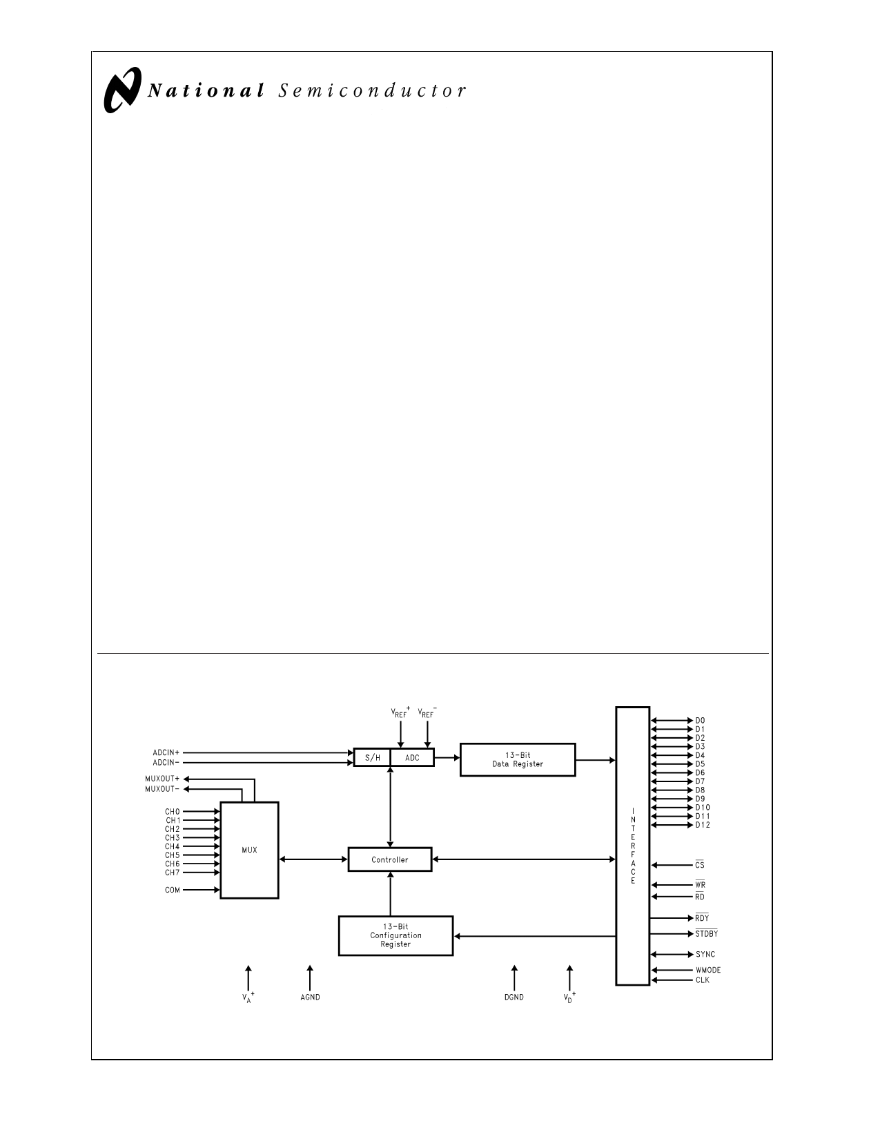
Block Diagram
TRI-STATE® is a registered trademark of National Semiconductor Corporation.
© 2000 National Semiconductor Corporation DS012387
DS012387-1
www.national.com
1 page 
Absolute Maximum Ratings (Notes 1, 2)
If Military/Aerospace specified devices are required,
please contact the National Semiconductor Sales Office/
Distributors for availability and specifications.
Supply Voltage (VA+ and VD+)
Voltage at all Inputs
|VA+ − VD+|
|AGND − DGND|
Input Current at Any Pin (Note 3)
Package Input Current (Note 3)
Power Dissipation (Note 4)
at TA = 25˚C
Storage Temperature
6.0V
−0.3V to V+ + 0.3V
300 mV
300 mV
±30 mA
±120 mA
875 mW
−65˚C to +150˚C
Lead Temperature
VF Package
Vapor Phase (60 sec.)
Infared (15 sec.)
V Package, Infared (15 sec.)
ESD Susceptibility (Note 5)
210˚C
220˚C
300˚C
3.0 kV
Operating Ratings (Notes 1, 2, 6, 7, 8, 9)
Temperature Range
(Tmin ≤ TA ≤ Tmax)
Supply Voltage
VA+, VD+
|VA+ − VD+|
|AGND − DGND|
VIN Voltage Range
at all Inputs
VREF+ Input Voltage
VREF− Input Voltage
VREF+ − VREF−
VREF Common Mode
(Note 16)
−40˚C ≤ TA ≤ 85˚C
4.5V to 5.5V
≤100 mV
≤100 mV
GND ≤ VIN ≤ VA+
1V ≤ VREF+ ≤ VA+
0 ≤ VREF− ≤ VREF+ − 1V
1V ≤ VREF ≤ VA+
0.1 VA+ ≤ VREFCM ≤ 0.6 VA+
Converter DC Characteristics
The following specifications apply to the ADC12048 for VA+ = VD+ = 5V, VREF+ = 4.096V, VREF− = 0.0V, 12-bit + sign conver-
sion mode, fCLK = 12.0 MHz, RS = 25Ω, source impedance for VREF+ and VREF− ≤ 1Ω, fully differential input with fixed 2.048V
common-mode voltage (VINCM), and minimum acquisition time, unless otherwise specified. Boldface limits apply for TA = TJ
= TMIN to TMAX; all other limits TA = TJ = 25˚C
Symbol
Parameter
Conditions
Typical
Limits
Unit
(Note 10)
(Note 11)
(Limit)
Resolution with No Missing
Codes
After Auto-Cal
13 Bits (max)
ILE Integral Linearity Error
After Auto-Cal
(Notes 12, 17)
±0.6
±1 LSB (max)
DNL
Differential Non-Linearity
Zero Error
TUE
Positive Full-Scale Error
Negative Full-Scale Error
DC Common Mode Error
Total Unadjusted Error
After Auto-Cal
After Auto-Cal (Notes 13, 17)
VINCM = 5.0V
VINCM = 2.048V
VINCM = 0V
After Auto-Cal (Notes 12, 17)
After Auto-Cal (Notes 12, 17)
After Auto-Cal (Note 14)
After Auto-Cal (Note 18)
±1.0
±1.0
±2
±1
±1
±5.5
±2.5
±5.5
±2.5
±2.5
±5.5
LSB (max)
LSB (max)
LSB (max)
LSB (max)
LSB (max)
LSB (max)
LSB (max)
LSB
Power Supply Characteristics
The following specifications apply to the ADC12048 for VA+ = VD+ = 5V, VREF+ = 4.096V, VREF− = 0.0V, 12-bit + sign conver-
sion mode, fCLK = 12.0 MHz, RS = 25Ω, source impedance for VREF+ and VREF− ≤ 1Ω, fully differential input with fixed 2.048V
common-mode voltage, and minimum acquisition time, unless otherwise specified. Boldface limits apply for TA = TJ = TMIN
to TMAX; all other limits TA = TJ = 25˚C
Symbol
Parameter
Conditions
Typical
Limits
Unit
(Note 10)
(Note 11)
(Limit)
PSS
Power Supply Sensitivity
Zero Error
Full-Scale Error
Linearity Error
VD+ = VA+ = 5.0V ±10% (Note 15)
VREF+ = 4.096V
VREF− = 0V
±0.1
±0.5
±0.1
LSB
LSB
LSB
5 www.national.com
5 Page 
Electrical Characteristics (Continued)
FIGURE 4. VREF Operating Range for VA = 5V
DS012387-8
FIGURE 5. Transfer Characteristic
11
DS012387-9
www.national.com
11 Page | ||
| Páginas | Total 30 Páginas | |
| PDF Descargar | [ Datasheet ADC12048EVAL.PDF ] | |
Hoja de datos destacado
| Número de pieza | Descripción | Fabricantes |
| ADC12048EVAL | 12-Bit Plus Sign 216 kHz 8-Channel Sampling Analog-to-Digital Converter | National Semiconductor |
| Número de pieza | Descripción | Fabricantes |
| SLA6805M | High Voltage 3 phase Motor Driver IC. |
Sanken |
| SDC1742 | 12- and 14-Bit Hybrid Synchro / Resolver-to-Digital Converters. |
Analog Devices |
|
DataSheet.es es una pagina web que funciona como un repositorio de manuales o hoja de datos de muchos de los productos más populares, |
| DataSheet.es | 2020 | Privacy Policy | Contacto | Buscar |