|
|
|
PDF ADC12020EVAL Data sheet ( Hoja de datos )
| Número de pieza | ADC12020EVAL | |
| Descripción | 12-Bit/ 20 MSPS/ 185 mW A/D Converter with Internal Sample-and-Hold | |
| Fabricantes | National Semiconductor | |
| Logotipo | ||
Hay una vista previa y un enlace de descarga de ADC12020EVAL (archivo pdf) en la parte inferior de esta página. Total 23 Páginas | ||
|
No Preview Available !
April 2003
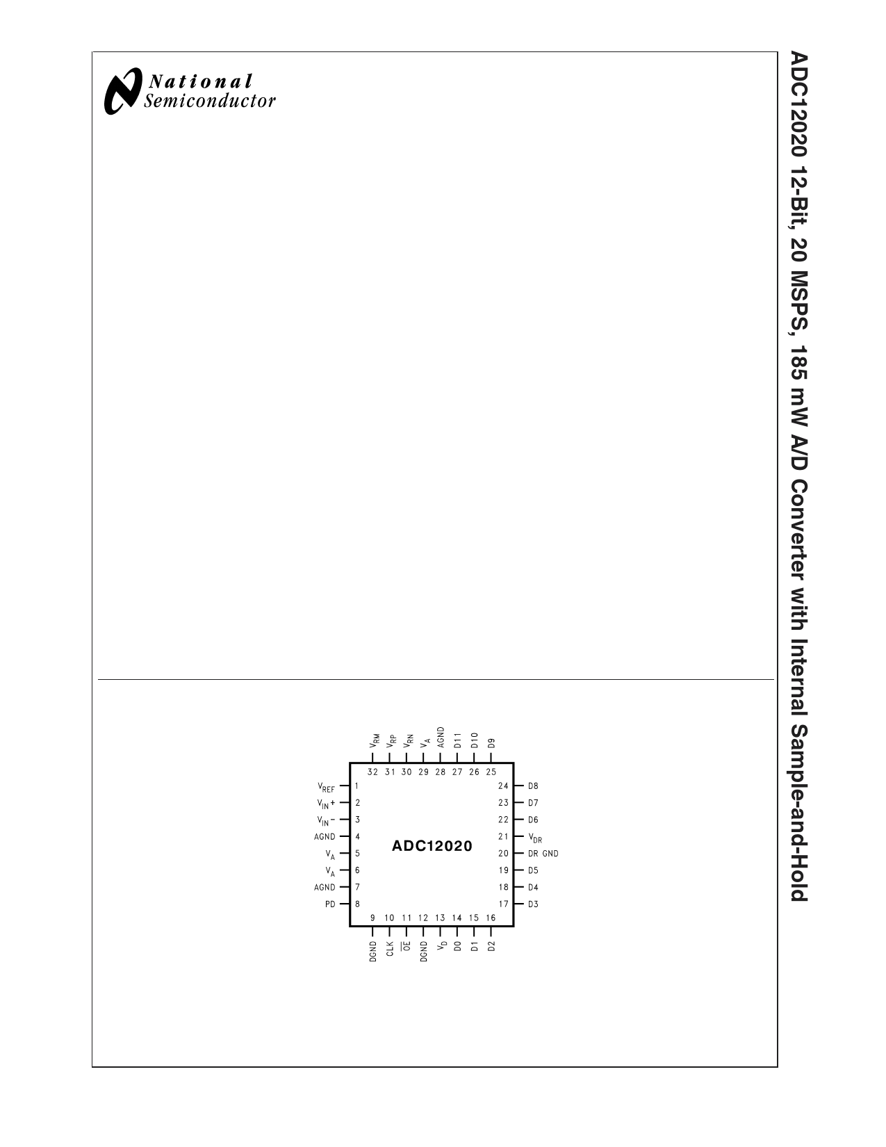
ADC12020
12-Bit, 20 MSPS, 185 mW A/D Converter with Internal
Sample-and-Hold
General Description
The ADC12020 is a monolithic CMOS analog-to-digital con-
verter capable of converting analog input signals into 12-bit
digital words at 20 Megasamples per second (MSPS), mini-
mum. This converter uses a differential, pipeline architecture
with digital error correction and an on-chip sample-and-hold
circuit to minimize die size and power consumption while
providing excellent dynamic performance. Operating on a
single 5V power supply, this device consumes just 185 mW
at 20 MSPS, including the reference current. The Power
Down feature reduces power consumption to 40 mW.
The differential inputs provide a full scale input swing equal
to 2VREF with the possibility of a single-ended input. Full use
of the differential input is recommended for optimum perfor-
mance. For ease of use, the buffered, high impedance,
single-ended reference input is converted on-chip to a differ-
ential reference for use by the processing circuitry. Output
data format is 12-bit offset binary.
This device is available in the 32-lead LQFP package and
will operate over the industrial temperature range of −40˚C to
+85˚C.
Features
n Internal sample-and-hold
n Outputs 2.5V to 5V compatible
n TTL/CMOS compatible input/outputs
n Power down mode
n On-chip reference buffer
Key Specifications
n Resolution
n Conversion Rate
n DNL
n INL
n SNR (fIN = 10.1 MHz)
n ENOB (fIN = 10.1 MHz)
n Data Latency
n Supply Voltage
n Power Consumption, 20 MHz
Applications
n Image Processing Front End
n Instrumentation
n PC-Based Data Acquisition
n Fax Machines
n Waveform Digitizers
n Sonar/Radar
n DSP Front Ends
12 Bits
20 MSPS (min)
±0.35 LSB (typ)
±0.55 LSB (typ)
70 dB (typ)
11.3 bits (typ)
6 Clock Cycles
+5V ±5%
185 mW (typ)
Connection Diagram
TRI-STATE® is a registered trademark of National Semiconductor Corporation.
© 2003 National Semiconductor Corporation DS200517
20051701
www.national.com
1 page 
Absolute Maximum Ratings (Notes 1,
2)
If Military/Aerospace specified devices are required,
please contact the National Semiconductor Sales Office/
Distributors for availability and specifications.
VA, VD
VDR
|VA–VD|
Voltage on Any Input or Output Pin
Input Current at Any Pin (Note 3)
Package Input Current (Note 3)
Package Dissipation at TA = 25˚C
ESD Susceptibility
Human Body Model (Note 5)
Machine Model (Note 5)
Soldering Temperature,
Infrared, 10 sec. (Note 6)
Storage Temperature
6.5V
≤VD+0.3V
≤ 100 mV
−0.3V to (VA or VD
+ 0.3V)
±25 mA
±50 mA
See (Note 4)
2500V
250V
235˚C
−65˚C to +150˚C
Operating Ratings (Notes 1, 2)
Operating Temperature
Supply Voltage (VA, VD)
Output Driver Supply (VDR)
VREF Input
CLK, PD, OE
VIN Input
VCM
|AGND–DGND|
−40˚C ≤ TA ≤ +85˚C
+4.75V to +5.25V
+2.35V to VD
1.0V to 2.4V
−0.05V to (VD + 0.05V)
−0V to (VA − 0.5V)
1.0V to 4.0V
≤100mV
Converter Electrical Characteristics
Unless otherwise specified, the following specifications apply for AGND = DGND = DR GND = 0V, VA = VD = +5V, VDR =
+3.0V, PD = 0V, VREF = +2.0V, fCLK = 20 MHz, tr = tf = 3 ns, CL = 25 pF/pin. Boldface limits apply for TA = TJ = TMIN to
TMAX: all other limits TA = TJ = 25˚C (Notes 7, 8, 9)
Symbol
Parameter
Conditions
Typical Limits
(Note 10) (Note 10)
Units
(Limits)
STATIC CONVERTER CHARACTERISTICS
Resolution with No Missing Codes
12 Bits (min)
INL Integral Non Linearity (Note 11)
±0.55
+1.7
-1.4
LSB (max)
LSB (min)
DNL
Differential Non Linearity
±0.35
+0.9
-1.0
LSB (max)
LSB (min)
GE Gain Error
±0.05
2.9 %FS (max)
Offset Error (VIN+ = VIN−)
Under Range Output Code
−0.04
0
±1.75
0
%FS (max)
Over Range Output Code
4095
4095
DYNAMIC CONVERTER CHARACTERISTICS
FPBW Full Power Bandwidth
0 dBFS Input, Output at −3 dB
100
MHz
SNR
Signal-to-Noise Ratio
SINAD Signal-to-Noise and Distortion
ENOB Effective Number of Bits
THD
Total Harmonic Distortion
fIN = 1 MHz, VIN = −0.5 dBFS
fIN = 4.4 MHz, VIN = −0.5 dBFS
fIN = 10.1 MHz, VIN = −0.5 dBFS
fIN = 1 MHz, VIN = −0.5 dBFS
fIN = 4.4 MHz, VIN = −0.5 dBFS
fIN = 10.1MHz, VIN = −0.5 dBFS
fIN = 1 MHz, VIN = −0.5 dBFS
fIN = 4.4 MHz, VIN = −0.5 dBFS
fIN = 10.1 MHz, VIN = −0.5 dBFS
fIN = 1 MHz, VIN = −0.5 dBFS
fIN = 4.4 MHz, VIN = −0.5 dBFS
fIN = 10.1 MHz,
+25˚C
VIN = −0.5 dBFS
+85˚C
70
70
70
70
70
69
11.3
11.3
11.3
−83
−83
−83
67
67
10.8
-74
-71
dB
dB
dB(min)
dB
dB
dB (min)
dB
dB
dB(min)
dB
dB
dB (min)
dB (min)
5 www.national.com
5 Page 
ADC12020 Typical Performance Characteristics VA = VD = 5V, VDR = 3.0V, fCLK = 20 MHz,
fIN = 10.1 MHz, VREF = 2.0V unless otherwise stated
DNL
DNL vs. Temperature
20051718
DNL vs. Clock Duty Cycle
DNL vs. Sample Rate
20051719
INL
20051720
INL vs. Temperature
20051721
20051722
11
20051723
www.national.com
11 Page | ||
| Páginas | Total 23 Páginas | |
| PDF Descargar | [ Datasheet ADC12020EVAL.PDF ] | |
Hoja de datos destacado
| Número de pieza | Descripción | Fabricantes |
| ADC12020EVAL | 12-Bit/ 20 MSPS/ 185 mW A/D Converter with Internal Sample-and-Hold | National Semiconductor |
| Número de pieza | Descripción | Fabricantes |
| SLA6805M | High Voltage 3 phase Motor Driver IC. |
Sanken |
| SDC1742 | 12- and 14-Bit Hybrid Synchro / Resolver-to-Digital Converters. |
Analog Devices |
|
DataSheet.es es una pagina web que funciona como un repositorio de manuales o hoja de datos de muchos de los productos más populares, |
| DataSheet.es | 2020 | Privacy Policy | Contacto | Buscar |