|
|
|
PDF ADC10832CIN Data sheet ( Hoja de datos )
| Número de pieza | ADC10832CIN | |
| Descripción | 10-Bit Plus Sign Serial I/O A/D Converters with MUX/ Sample/Hold and Reference | |
| Fabricantes | National Semiconductor | |
| Logotipo | ||
Hay una vista previa y un enlace de descarga de ADC10832CIN (archivo pdf) en la parte inferior de esta página. Total 30 Páginas | ||
|
No Preview Available !
December 1994
ADC10831 ADC10832 ADC10834 ADC10838
10-Bit Plus Sign Serial I O A D Converters
with MUX Sample Hold and Reference
General Description
This series of CMOS 10-bit plus sign successive approxima-
tion A D converters features versatile analog input multi-
plexers sample hold and a 2 5V band-gap reference The
1 2 4 or 8-channel multiplexers can be software configured
for single-ended or differential mode of operation
An input sample hold is implemented by a capacitive refer-
ence ladder and sampled-data comparator This allows the
analog input to vary during the A D conversion cycle
In the differential mode valid outputs are obtained even
when the negative inputs are greater than the positive be-
cause of the 10-bit plus sign output data format
The serial I O is configured to comply with the NSC
MICROWIRETM serial data exchange standard for easy in-
terface to the COPSTM and HPCTM families of controllers
and can easily interface with standard shift registers and
microprocessors
Applications
Y Medical instruments
Y Remote instrumentation
Y Test equipment
Features
Y b5V to a5V analog voltage range with g5V supplies
Y Serial I O (MICROWIRE compatible)
Y 1 2 4 or 8-channel differential or single-ended
multiplexer
Y Software or hardware power down
Y Analog input sample hold function
Y Ratiometric or Absolute voltage referencing
Y No zero or full scale adjustment required
Y No missing codes over temperature
Y TTL MOS input output compatible
Y Standard DIP and SO packages
Key Specifications
Y Resolution
Y Dual supply
Y Power dissipation
Y In power down mode
Y Conversion time
Y Sampling rate
Y Band-gap reference
10 bits plus sign
g5V
59 mW (Max)
33 mW
5 ms (Max)
74 kHz (Max)
2 5V g2% (Max)
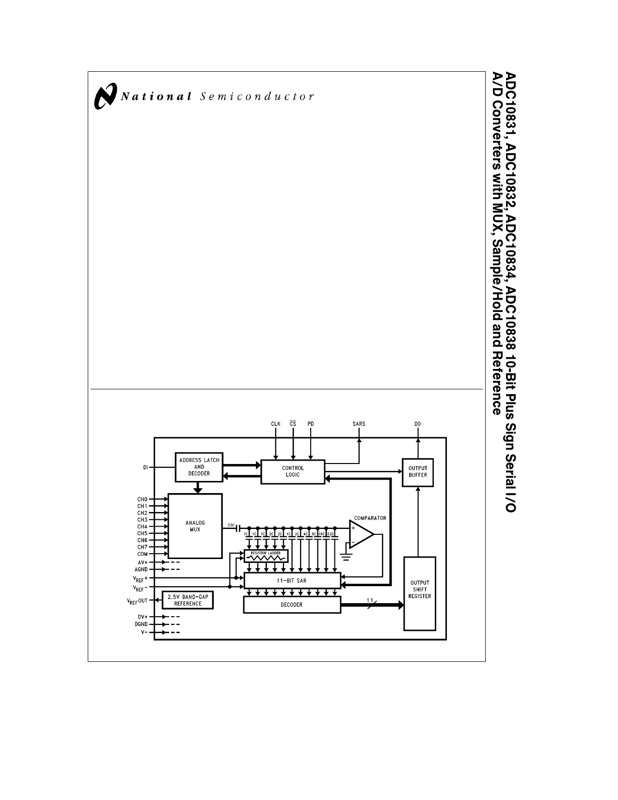
ADC10838 Simplified Block Diagram
COPSTM HPCTM and MICROWIRETM are trademarks of National Semiconductor Corporation
C1995 National Semiconductor Corporation TL H 11391
TL H 11391 – 1
RRD-B30M75 Printed in U S A
1 page 
Electrical Characteristics (Continued)
The following specifications apply for Va e AVa e DVa e a5 0 VDC VREFa e a4 096 VDC VREFb e VINb e GND
Vb e b5 0 VDC and fCLK e 2 5 MHz unless otherwise specified Boldface limits apply for TA e TJ e TMIN to TMAX
all other limits TA e TJ e a25 C (Notes 8 9 and 10) (Continued)
Symbol
Parameter
Conditions
Typical
(Note 11)
Limits
(Note 12)
Units
(Limits)
REFERENCE CHARACTERISTICS
VREFOut
DVREF DT
DVREF DIL
DVREF DIL
Reference Output Voltage
VREFOut Temperature Coefficient
Load Regulation Sourcing
Load Regulation Sinking
Line Regulation
0 mA s IL s a4 mA
0 mA s IL s b1 mA
5V g10%
2 5V g0 5%
g40
g0 003
g0 2
g0 3
2 5V g2%
g0 05
g0 6
g2 5
V(max)
ppm C
% mA(max)
% mA(max)
mV(max)
ISC Short Circuit Current
Noise Voltage
DVREF Dt Long-term Stability
tSU Start-Up Time
DIGITAL AND DC CHARACTERISTICS
VREFOut e 0V
10 Hz to 10 kHz CL e 100 mF
CL e 100 mF
13
5
g120
100
22 mA(max)
mV
ppm kHr
ms
VIN(1)
VIN(0)
IIN(1)
IIN(0)
VOUT(1)
VOUT(0)
IOUT
aISC
Logical ‘‘1’’ Input Voltage
Logical ‘‘0’’ Input Voltage
Logical ‘‘1’’ Input Current
Logical ‘‘0’’ Input Current
Logical ‘‘1’’ Output Voltage
Logical ‘‘0’’ Output Voltage
TRI-STATE Output Current
Output Short-Circuit Source
Current
Va e 5 5V
Va e 4 5V
VIN e 5 0V
VIN e 0V
Va e 4 5V IOUT e b360 mA
Va e 4 5V IOUT e b10 mA
Va e 4 5V IOUT e 1 6 mA
VOUT e 0V
VOUT e 5V
VOUT e 0V Va e 4 5V
0 005
b0 005
b0 1
a0 1
b30
20
08
a2 5
b2 5
24
45
04
b3 0
a3 0
b15
V(min)
V(max)
mA(max)
mA(min)
V(min)
V(min)
V(min)
mA(min)
mA(max)
mA(max)
bISC
Output Short-Circuit Sink Current VOUTe Va e 4 5V
30 15 mA(min)
IDa Digital Supply Current
(Note 17)
CS e HIGH Power Up
0 9 1 3 mA(max)
CS e HIGH Power Down 0 2 0 4 mA(max)
CS e HIGH Power Down 0 5 50 mA(max)
and CLK Off
IAa
Positive Analog Supply Current
CS e HIGH Power Up
2 7 6 0 mA(max)
(Note 17)
CS e HIGH Power Down 3 0 15 mA(max)
IAb Negative Analog Supply Current CS e HIGH Power Up
(Note 17)
CS e HIGH Power Down
b2 7
b3 0
b4 5
b15
mA(min)
mA(min)
IREF
Reference Input Current
VREFa e a2 5V and
CS e HIGH Power Up
0 6 mA(max)
5
5 Page 
Typical Reference Performance Characteristics
Load Regulation
Line Regulation
Output Drift
vs Temperature
(3 Typical Parts)
Available
Output Current
vs Supply Voltage
TL H 11391 – 11
11
11 Page | ||
| Páginas | Total 30 Páginas | |
| PDF Descargar | [ Datasheet ADC10832CIN.PDF ] | |
Hoja de datos destacado
| Número de pieza | Descripción | Fabricantes |
| ADC10832CIN | 10-Bit Plus Sign Serial I/O A/D Converters with MUX/ Sample/Hold and Reference | National Semiconductor |
| ADC10832CIWM | 10-Bit Plus Sign Serial I/O A/D Converters with MUX/ Sample/Hold and Reference | National Semiconductor |
| Número de pieza | Descripción | Fabricantes |
| SLA6805M | High Voltage 3 phase Motor Driver IC. |
Sanken |
| SDC1742 | 12- and 14-Bit Hybrid Synchro / Resolver-to-Digital Converters. |
Analog Devices |
|
DataSheet.es es una pagina web que funciona como un repositorio de manuales o hoja de datos de muchos de los productos más populares, |
| DataSheet.es | 2020 | Privacy Policy | Contacto | Buscar |