|
|
PDF ADC10158 Data sheet ( Hoja de datos )
| Número de pieza | ADC10158 | |
| Descripción | 10-Bit Plus Sign 4 s ADCs with 4- or 8-Channel MUX/ Track/Hold and Reference | |
| Fabricantes | National Semiconductor | |
| Logotipo | ||
Hay una vista previa y un enlace de descarga de ADC10158 (archivo pdf) en la parte inferior de esta página. Total 23 Páginas | ||
|
No Preview Available !
November 1999
ADC10154/ADC10158
10-Bit Plus Sign 4 µs ADCs with 4- or 8-Channel MUX,
Track/Hold and Reference
General Description
The ADC10154 and ADC10158 are CMOS 10-bit plus sign
successive approximation A/D converters with versatile ana-
log input multiplexers, track/hold function and a 2.5V
band-gap reference. The 4-channel or 8-channel multiplex-
ers can be software configured for single-ended, differential
or pseudo-differential modes of operation.
The input track/hold is implemented using a capacitive array
and sampled-data comparator.
Resolution can be programmed to be 8-bit, 8-bit plus sign,
10-bit or 10-bit plus sign. Lower-resolution conversions can
be performed faster.
The variable resolution output data word is read in two bytes,
and can be formatted left justified or right justified, high byte
first.
Applications
n Process control
n Instrumentation
n Test equipment
Features
n 4- or 8- channel configurable multiplexer
n Analog input track/hold function
n 0V to 5V analog input range with single +5V power
supply
n −5V to +5V analog input voltage range with ±5V
supplies
n Fully tested in unipolar (single +5V supply) and bipolar
(dual ±5V supplies) operation
n Programmable resolution/speed and output data format
n Ratiometric or Absolute voltage reference operation
n No zero or full scale adjustment required
n No missing codes over temperature
n Easy microprocessor interface
Key Specifications
n Resolution
n Integral linearity error
n Unipolar power dissipation
n Conversion time (10-bit + sign)
n Conversion time (8-bit)
n Sampling rate (10-bit + sign)
n Sampling rate (8-bit)
n Band-gap reference
10-bit plus sign
±1 LSB (max)
33 mW (max)
4.4 µs (max)
3.2 µs (max)
166 kHz
207 kHz
2.5V ±2.0% (max)
ADC10158 Simplified Block Diagram
TRI-STATE® is a registered trademark of National Semiconductor Corporation.
© 1999 National Semiconductor Corporation DS011225
DS011225-1
www.national.com
1 page 
Electrical Characteristics (Continued)
The following specifications
operation or V− = −5.0 VDC
apply for V+ = AV+ =
for bipolar operation,
DV+ = +
and fCLK
=5.05.0VDMCH, zVRuEnFle+s=s
5.000 VDC, VREF− =
otherwise specified.
GND, V−
Boldface
= GND for unipolar
limits apply for TA
= TJ = TMIN to TMAX; all other limits TA = TJ = 25˚C. (Notes 8, 9, 12)
Symbol
Parameter
Conditions
Typical
(Note 10)
Limits
(Note 11)
Units
(Limit)
DYNAMIC CONVERTER AND MULTIPLEXER CHARACTERISTICS
−3 dB Unipolar Full
Power Bandwidth
VIN = 4.85 Vp–p
200
kHz
−3 dB Bipolar Full
Power Bandwidth
VIN = ±4.85V
200 kHz
REFERENCE CHARACTERISTICS (Unipolar Operation V− = GND Only)
VREFOut Reference Output Voltage
2.5 ±1% 2.5 ± 2%
V (Max)
∆VREF/∆t
∆VREF/∆IL
VREFOut Temperature Coefficient
Load Regulation Sourcing
Sinking
Line Regulation
0 mA ≤ IL ≤ +4 mA
0 mA ≥ IL ≥ −1 mA
4.5V ≤ V+ ≤ 5.5V
40
0.003
0.2
0.5
ppm/˚C
0.1 %/mA (Max)
0.6 %/mA (Max)
6 mV (Max)
ISC Short Circuit Current
∆VREF/∆t Long-Term Stability
tSU Start-Up Time
DIGITAL AND DC CHARACTERISTICS
VREFOut = 0V
CL = 330 µF
14 25 mA (Max)
200 ppm/1 kHr
20 ms
VIN(1)
VIN(0)
IIN(1)
IIN(0)
VOUT(1)
VOUT(0)
IOUT
+ISC
−ISC
Logical “1” Input Voltage
Logical “0” Input Voltage
Logical “1” Input Current
Logical “0” Input Current
Logical “1” Output Voltage
Logical “0” Output Voltage
TRI-STATE® Output Current
Output Short Circuit Source Current
Output Short Circuit
Sink Current
V+ = 5.5V
V+ = 4.5V
VIN = 5.0V
VIN = 0V
V+ = 4.5V:
V+ = 4.5V
IOUT = 1.6 mA
VOUT = 0V
VOUT = 5V
VOUT = 0V
VOUT = DV+
IOUT = −360 µA
IOUT = −10 µA
0.005
−0.005
−0.01
0.01
−40
30
2.0
0.8
2.5
−2.5
2.4
4.25
0.4
−3
3
−10
10
V (Min)
V (Max)
µA (Max)
µA (Max)
V (Min)
V (Min)
V (Max)
µA (Max)
µA (Max)
mA (Min)
mA (Min)
DI+ Digital Supply Current
CS = HIGH
0.75
2 mA (Max)
AI+ Analog Supply Current
CS = HIGH, fCLK = 0 Hz
CS = HIGH
0.15
mA (Max)
3 4.5 mA (Max)
I− Negative Supply Current
CS = HIGH, fCLK = 0 Hz
CS = HIGH
3 mA (Max)
3.5 4.5 mA (Max)
IREF Reference Input Current
CS = HIGH, fCLK = 0 Hz
VREF+ = 5V
3.5 mA (Max)
0.7 1.1 mA (Max)
5 www.national.com
5 Page 
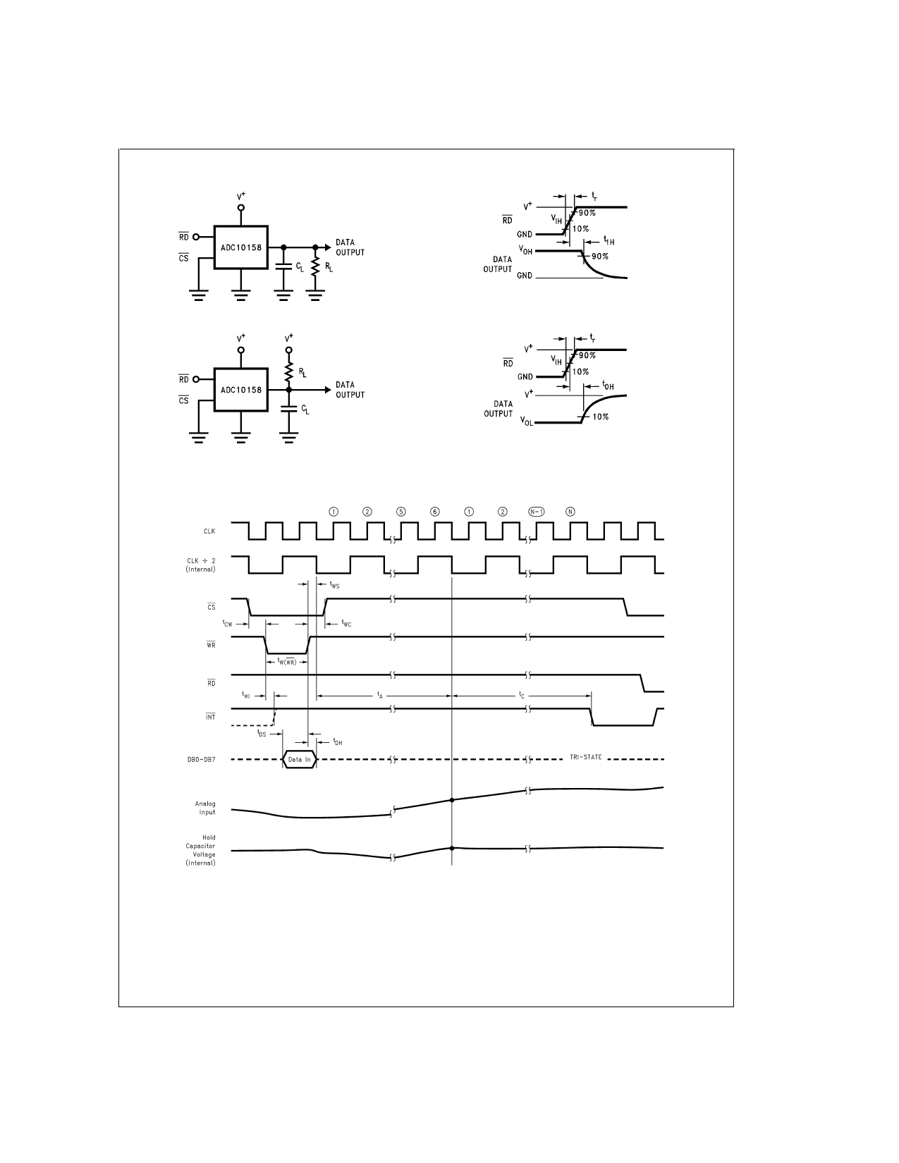
TRI-STATE Test Circuits and Waveforms
DS011225-11
Timing Diagrams
DS011225-13
DS011225-12
DS011225-14
DS011225-15
DIAGRAM 1. Starting a Conversion with New MUX Channel and Output Configuration
11 www.national.com
11 Page | ||
| Páginas | Total 23 Páginas | |
| PDF Descargar | [ Datasheet ADC10158.PDF ] | |
Hoja de datos destacado
| Número de pieza | Descripción | Fabricantes |
| ADC10154 | 10-Bit Plus Sign 4 s ADCs with 4- or 8-Channel MUX/ Track/Hold and Reference | National Semiconductor |
| ADC10154 | ADC10154/58 10-Bit + 4 ADCs with 4 or 8-Channel MUX Track/Hold and Ref (Rev. A) | Texas Instruments |
| ADC10154CIWM | 10-Bit Plus Sign 4 s ADCs with 4- or 8-Channel MUX/ Track/Hold and Reference | National Semiconductor |
| ADC10158 | 10-Bit Plus Sign 4 s ADCs with 4- or 8-Channel MUX/ Track/Hold and Reference | National Semiconductor |
| Número de pieza | Descripción | Fabricantes |
| SLA6805M | High Voltage 3 phase Motor Driver IC. |
Sanken |
| SDC1742 | 12- and 14-Bit Hybrid Synchro / Resolver-to-Digital Converters. |
Analog Devices |
|
DataSheet.es es una pagina web que funciona como un repositorio de manuales o hoja de datos de muchos de los productos más populares, |
| DataSheet.es | 2020 | Privacy Policy | Contacto | Buscar |
