|
|
|
PDF ADC08D1000 Data sheet ( Hoja de datos )
| Número de pieza | ADC08D1000 | |
| Descripción | High Performance/ Low Power/ Dual 8-Bit/ 1 GSPS A/D Converter | |
| Fabricantes | National Semiconductor | |
| Logotipo | ||
Hay una vista previa y un enlace de descarga de ADC08D1000 (archivo pdf) en la parte inferior de esta página. Total 30 Páginas | ||
|
No Preview Available !
ADVANCE INFORMATION
September 2004
ADC08D1000
High Performance, Low Power, Dual 8-Bit, 1 GSPS A/D
Converter
General Description
NOTE: This product is currently in development. – ALL
specifications are design targets and are subject to
change.
The ADC08D1000 is a dual, low power, high performance
CMOS analog-to-digital converter that digitizes signals to 8
bits resolution at sampling rates up to 1.6 GSPS. Consuming
a typical 1.6 Watts at 1 GSPS from a single 1.9 Volt supply,
this device is guaranteed to have no missing codes over the
full operating temperature range. The unique folding and
interpolating architecture, the fully differential comparator
design, the innovative design of the internal sample-and-
hold amplifier and the self-calibration scheme enable a very
flat response of all dynamic parameters beyond Nyquist,
producing a high 7.5 ENOB with a 500 MHz input signal and
a 1 GHz sample rate while providing a 10-18 B.E.R. Output
formatting is offset binary and the LVDS digital outputs are
compliant with IEEE 1596.3-1996, with the exception of a
reduced common mode voltage of 0.8V.
Each converter has a 1:2 demultiplexer that feeds two LVDS
buses and reduces the output data rate on each bus to half
the sampling rate. The two converters can be interleaved
and used as a single 2 GSPS ADC.
The converter typically consumes less than 20 mW in the
Power Down Mode and is available in a 128-lead, thermally
enhanced exposed pad LQFP and operates over the indus-
trial (-40˚C ≤ TA ≤ +85˚C) temperature range.
Features
n Internal Sample-and-Hold
n Single +1.9V ±0.1V Operation
n Choice of SDR or DDR output clocking
n Interleave Mode for 2x Sampling Rate
n Multiple ADC Synchronization Capability
n Guaranteed No Missing Codes
n Serial Interface for Extended Control
n Fine Adjustment of Input Full-Scale Range and Offset
Key Specifications
n Resolution
n Max Conversion Rate
n Bit Error Rate
n ENOB @ 500 MHz Input
n DNL
n Power Consumption
— Operating
— Power Down Mode
8 Bits
1 GSPS (min)
10-18 (typ)
7.5 Bits (typ)
±0.25 LSB (typ)
1.6 W (typ)
20 mW (typ)
Applications
n Direct RF Down Conversion
n Digital Oscilloscopes
n Satellite Set-top boxes
n Communications Systems
n Test Instrumentation
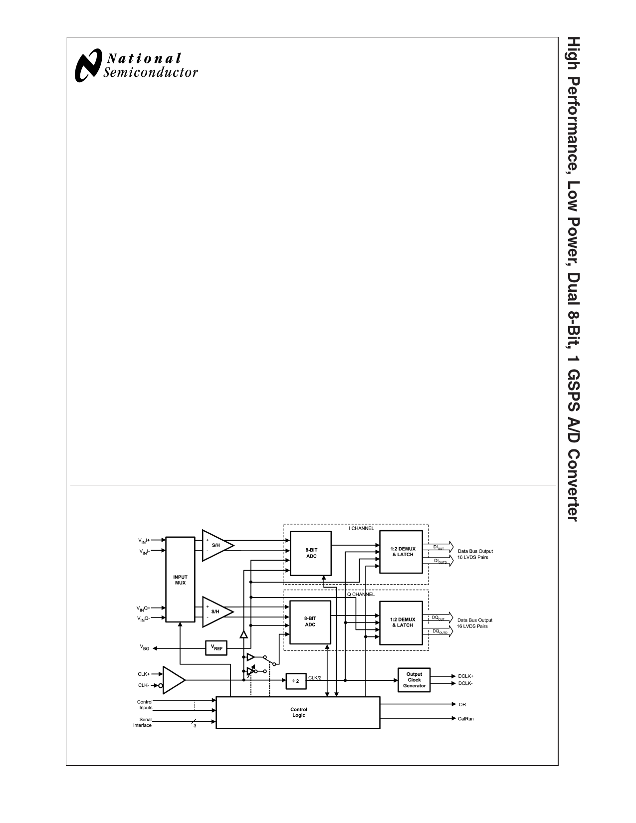
Block Diagram
© 2004 National Semiconductor Corporation DS200974
20097453
www.national.com
1 page 
Pin Descriptions and Equivalent Circuits (Continued)
Pin Functions
Pin No.
Symbol
83 / 78 DI7− / DQ7−
84 / 77 DI7+ / DQ7+
85 / 76 DI6− / DQ6−
86 / 75 DI6+ / DQ6+
89 / 72 DI5− / DQ5−
90 / 71 DI5+ / DQ5+
91 / 70 DI4− / DQ4−
92 / 69 DI4+ / DQ4+
93 / 68 DI3− / DQ3−
94 / 67 DI3+ / DQ3+
95 / 66 DI2− / DQ2−
96 / 65 DI2+ / DQ2+
100 / 61 DI1− / DQ1−
101 / 60 DI1+ / DQ1+
102 / 59 DI0− / DQ0−
103 / 58 DI0+ / DQ0+
104 / 57 DId7− / DQd7−
105 / 56 DId7+ / DQd7+
106 / 55 DId6− / DQd6−
107 / 54 DId6+ / DQd6+
111 / 50 DId5− / DQd5−
112 / 49 DId5+ / DQd5+
113 / 48 DId4− / DQd4−
114 / 47 DId4+ / DQd4+
115 / 46 DId3− / DQd3−
116 / 45 DId3+ / DQd3+
117 / 44 DId2− / DQd2−
118 / 43 DId2+ / DQd2+
122 / 39 DId1− / DQd1−
123 / 38 DId1+ / DQd1+
124 / 37 DId0− / DQd0−
125 / 36 DId0+ / DQd0+
Equivalent Circuit
Description
I and Q channel LVDS Data Outputs that are not delayed in
the output demultiplexer. Compared with the DId and DQd
outputs, these outputs represent the later time samples.
These outputs should always be terminated with a 100Ω
differential resistor.
I and Q channel LVDS Data Outputs that are delayed by one
CLK cycle in the output demultiplexer. Compared with the
DI/DQ outputs, these outputs represent the earlier time
sample. These outputs should always be terminated with a
100Ω differential resistor.
79 OR+
80 OR-
Out Of Range output. A differential high at these pins
indicates that the differential input is out of range (outside the
range ±300 mV or ±400 mV as defined by the FSR pin).
82 DCLK+
81 DCLK-
2, 5, 8,
13, 16,
17, 20,
25, 28,
33, 128
VA
Differential Clock outputs used to latch the output data.
Delayed and non-delayed data outputs are supplied
synchronous to this signal. This signal is at 1/2 the input clock
rate in SDR mode and at 1/4 the input clock rate in the DDR
mode.
Analog power supply pins. Bypass these pins to ground.
5 www.national.com
5 Page 
Converter Electrical Characteristics (Continued)
[Note: This product is currently in development. As such, the parameters specified in this section are DESIGN TAR-
GETS. The specifications in this section cannot be guaranteed until device characterization has taken place.]
The following specifications apply after calibration for VA = VDR = +1.9VDC, OutV = 1.9V, VIN FSR (a.c. coupled) = differential
800mVP-P, CL = 10 pF, Differential, a.c. coupled Sinewave Input Clock, fCLK = 1 GHz at 0.5VP-P with 50% duty cycle, Non-
Extended Control Mode, REXT = 3300Ω ±0.1%, Analog Signal Source Impedance = 100Ω. Boldface limits apply for TA =
TMIN to TMAX. All other limits TA = 25˚C, unless otherwise noted. (Notes 6, 7)
Symbol
Parameter
Conditions
Typical
(Note 8)
Limits
(Note 8)
Units
(Limits)
AC ELECTRICAL CHARACTERISTICS
DI Outputs
13
DId Outputs
14
Normal Mode
13
Pipeline Delay (Latency)
(Note 11)
DQ Outputs
Extended
Control Mode
13.5
Input Clock
Cycles
Normal Mode
14
Over Range Recovery Time
DQd Outputs
Extended
Control Mode
Differential VIN step from ±1.2V to
0V to get accurate conversion
TBD
14.5
ns
PD low to Rated Accuracy
tWU Conversion (Wake-Up Time)
500 ns
fSCLK
tSSU
tSH
Maximum Serial Clock Frequency
Data to Serial Clock Setup Time
Data to Serial Clock Hold Time
Serial Clock Low Time
(Note 12)
(Note 12)
100 MHz
2.5
TBD
ns (min)
1
TBD
ns (min)
4 ns (min)
Serial Clock High Time
tCAL Calibration Cycle Time
4 ns (min)
1.4 x 10⁵
Clock Cycles
Note 1: Absolute Maximum Ratings indicate limits beyond which damage to the device may occur. There is no guarantee of operation at the Absolute Maximum
Ratings. Operating Ratings indicate conditions for which the device is functional, but do not guarantee specific performance limits. For guaranteed specifications and
test conditions, see the Electrical Characteristics. The guaranteed specifications apply only for the test conditions listed. Some performance characteristics may
degrade when the device is not operated under the listed test conditions.
Note 2: All voltages are measured with respect to GND = DR GND = 0V, unless otherwise specified.
Note 3: When the input voltage at any pin exceeds the power supply limits (that is, less than GND or greater than VA), the current at that pin should be limited to
25 mA. The 50 mA maximum package input current rating limits the number of pins that can safely exceed the power supplies with an input current of 25 mA to two.
This limit is not placed upon the power, ground and digital output pins.
Note 4: Human body model is 100 pF capacitor discharged through a 1.5 kΩ resistor. Machine model is 220 pF discharged through ZERO Ohms.
Note 5: See AN-450, “Surface Mounting Methods and Their Effect on Product Reliability”.
Note 6: The analog inputs are protected as shown below. Input voltage magnitudes beyond the Absolute Maximum Ratings may damage this device.
20097404
Note 7: To guarantee accuracy, it is required that VA and VDR be well bypassed. Each supply pin must be decoupled with separate bypass capacitors. Additionally,
achieving rated performance requires that the backside exposed pad be well grounded.
Note 8: Typical figures are at TJ = 25˚C, and represent most likely parametric norms. Test limits are guaranteed to National’s AOQL (Average Outgoing Quality
Level).
Note 9: Calculation of Full-Scale Error for this device assumes that the actual reference voltage is exactly its nominal value. Full-Scale Error for this device,
therefore, is a combination of Full-Scale Error and Reference Voltage Error. See Figure 2. For relationship between Gain Error and Full-Scale Error, see Specification
Definitions for Gain Error.
Note 10: The analog and clock input capacitances are die capacitances only. Additional package capacitances of 0.65 pF differential and 0.95 pF each pin to ground
are isolated from the die capacitances by lead and bond wire inductances.
Note 11: This parameter is guaranteed by design and is not tested in production.
11 www.national.com
11 Page | ||
| Páginas | Total 30 Páginas | |
| PDF Descargar | [ Datasheet ADC08D1000.PDF ] | |
Hoja de datos destacado
| Número de pieza | Descripción | Fabricantes |
| ADC08D1000 | High Performance/ Low Power/ Dual 8-Bit/ 1 GSPS A/D Converter | National Semiconductor |
| ADC08D1000 | ADC08D1000 High Performance Low Power Dual 8-Bit 1 GSPS A/D Converter (Rev. I) | Texas Instruments |
| ADC08D1000CIYB | High Performance/ Low Power/ Dual 8-Bit/ 1 GSPS A/D Converter | National Semiconductor |
| ADC08D1000EVAL | High Performance/ Low Power/ Dual 8-Bit/ 1 GSPS A/D Converter | National Semiconductor |
| Número de pieza | Descripción | Fabricantes |
| SLA6805M | High Voltage 3 phase Motor Driver IC. |
Sanken |
| SDC1742 | 12- and 14-Bit Hybrid Synchro / Resolver-to-Digital Converters. |
Analog Devices |
|
DataSheet.es es una pagina web que funciona como un repositorio de manuales o hoja de datos de muchos de los productos más populares, |
| DataSheet.es | 2020 | Privacy Policy | Contacto | Buscar |