|
|
|
PDF ADC08831IN Data sheet ( Hoja de datos )
| Número de pieza | ADC08831IN | |
| Descripción | 8-Bit Serial I/O CMOS A/D Converters with Multiplexer and Sample/Hold Function | |
| Fabricantes | National Semiconductor | |
| Logotipo | ||
Hay una vista previa y un enlace de descarga de ADC08831IN (archivo pdf) en la parte inferior de esta página. Total 23 Páginas | ||
|
No Preview Available !
September 1999
ADC08831/ADC08832
8-Bit Serial I/O CMOS A/D Converters with Multiplexer
and Sample/Hold Function
General Description
The ADC08831/ADC08832 are 8-bit successive approxima-
tion Analog to Digital converters with 3-wire serial interfaces
and a configurable input multiplexer for 2 channels. The se-
rial I/O will interface to COPS™family of micro-controllers,
PLD’s, microprocessors, DSP’s, or shift registers. The serial
I/O is configured to comply with the NSC MICROWIRE™ se-
rial data exchange standard.
To minimize total power consumption, the
ADC08831/ADC08832 automatically go into low power
mode whenever they are not performing conversions.
A track/hold function allows the analog voltage at the positive
input to vary during the actual A/D conversion.
The analog inputs can be configured to operate in various
combinations of single-ended, differential, or
pseudo-differential modes. The voltage reference input can
be adjusted to allow encoding of small analog voltage spans
to the full 8-bits of resolution.
Applications
n Digitizing sensors and waveforms
n Process control monitoring
n Remote sensing in noisy environments
n Instrumentation
n Embedded Systems
Features
n 3-wire serial digital data link requires few I/O pins
n Analog input track/hold function
n 2-channel input multiplexer option with address logic
n Analog input voltage range from GND to VCC
n No zero or full scale adjustment required
n TTL/CMOS input/output compatible
n Superior pin compatible replacement for ADC0831/2
Key Specifications
n Resolution: 8 bits
n Conversion time (fC = 2 MHz): 4µs (max)
n Power dissipation: 8.5mW (typ)
n Low power mode: 3.0mW (typ)
n Single supply: 5VDC
n Total unadjusted error: ±1LSB
n No missing codes over temperature
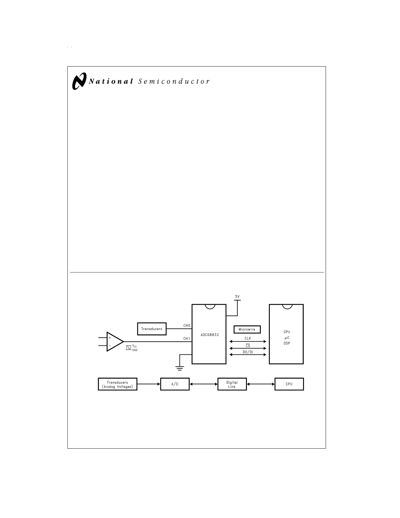
Typical Application
COPS™ is a trademark of National Semiconductor Corporation.
MICROWIRE™ is a trademark of National Semiconductor Corporation.
TRI-STATE™
© 1999 National Semiconductor Corporation DS100108
DS100108-44
DS100108-43
www.national.com
1 page 
Dynamic Characteristics
The following specifications apply for VCC = 5V, fCLK = 2MHz, TA= 25˚C, RSOURCE = 50Ω, fIN = 45kHz, VIN = 5VP, VREF = 5V,
non-coherent 2048 samples with windowing.
Symbol
Parameter
fS
SNR
THD
SINAD
ENOB
SFDR
Sampling Rate ADC08831
ADC08832
Signal-to -Noise Ratio (Note 19)
Total Harmonic Distortion (Note 20)
Signal-to -Noise and Distortion
Effective Number Of Bits (Note 18)
Spurious Free Dynamic Range
Conditions
fCLK/11
fCLK/13 (Note 21)
Typical
(Note 8)
48.5
−59.5
48.0
7.7
62.5
Limits
(Note 9)
181
153
Units
(Limits)
ksps
ksps
dB
dB
dB
Bits
dB
Note 1: Absolute Maximum Ratings indicate limits beyond which damage to the device may occur.
Note 2: Operating Ratings indicate conditions for which the device is functional. These ratings do not guarantee specific performance limits. For guaranteed speci-
fications and test conditions, see the Electrical Characteristics. The guaranteed specifications apply only for the test conditions listed. Some performance character-
istics may degrade when the device is not operated under the listed test conditions.
Note 3: All voltages are measured with respect to GND = 0 VDC, unless otherwise specified.
Note 4: When the input voltage VIN at any pin exceeds the power supplies (VIN < (GND) or VIN > VCC,) the current at that pin should be limited to 5 mA. The 20
mA maximum package input current rating limits the number of pins that can safely exceed the power supplies with an input current of 5 mA to four pins.
Note 5: The maximum power dissipation must be derated at elevated temperatures and is dictated by TJMAX, θJA and the ambient temperature, TA. The maximum
allowable power dissipation at any temperature is PD = (TJMAX − TA)/θJA or the number given in the Absolute Maximum Ratings, whichever is lower.
Note 6: Human body model, 100 pF capacitor discharged through a 1.5 kΩ resistor. The machine mode is a 200pF capacitor discharged directly into each pin.
Note 7: See AN450 “Surface Mounting Methods and Their Effect on Product Reliability” or Linear Data Book section “Surface Mount” for other methods of soldering
surface mount devices.
Note 8: Typicals are at TJ = 25˚C and represent the most likely parametric norm.
Note 9: Guaranteed to National’s AOQL (Average Outgoing Quality Level).
Note 10: Total Unadjusted Error (TUE) includes offset, full-scale, linearity, multiplexer errors.
Note 11: It is not tested for the ADC08832.
Note 12: For VIN(−) ≥ VIN(+) the digital code will be 0000 0000. Two on-chip diodes are tied to each analog input (see Functional Block Diagram) which will
forward-conduct for analog input voltages one diode drop below ground or one diode drop greater than VCC supply. During testing at low VCC levels (e.g., 4.5V), high
level analog inputs (e.g., 5V) can cause an input diode to conduct, especially at elevated temperatures, which will cause errors for analog inputs near full-scale. The
spec allows 50 mV forward bias of either diode; this means that as long as the analog VIN does not exceed the supply voltage by more than 50 mV, the output code
will be correct. Exceeding this range on an unselected channel will corrupt the reading of a selected channel. Achievement of an absolute 0 VDC to 5 VDC input voltage
range will therefore require a minimum supply voltage of 4.950 VDC over temperature variations, initial tolerance and loading.
Note 13: Channel leakage current is measured after a single-ended channel is selected and the clock is turned off. For off channel leakage current the following two
cases are considered: one, with the selected channel tied high (5 VDC) and the remaining off channel tied low (0 VDC), total current flow through the off channel is
measured; two, with the selected channel tied low and the off channels tied high, total current flow through the off channel is again measured. The two cases con-
sidered for determining on channel leakage current are the same except total current flow through the selected channel is measured.
Note 14: A 40% to 60% duty cycle range insures proper operation at all clock frequencies. In the case that an available clock has a duty cycle outside of these limits
the minimum time the clock is high or low must be at least 250 ns. The maximum time the clock can be high or low is 60 µs.
Note 15: Since data, MSB first, is the output of the comparator used in the successive approximation loop, an additional delay is built in to allow for comparator re-
sponse time.
Note 16: For the ADC08832 Vref is internally tied to VCC, therefore, for the ADC08832 reference current is included in the supply current.
Note 17: Analog inputs are typically 300 ohms input resistance to a 13pF sample and hold capacitor.
Note 18: Effective Number Of Bits (ENOB) is calculated from the measured signal-to-noise plus distortion ratio (SINAD) using the equation ENOB = (SINAD-1.76)/
6.02.
Note 19: The signal-to-noise ratio is the ratio of the signal amplitude to the background noise level. Harmonics of the input signal are not included in it’s calculation.
Note 20: The contributions from the first 6 harmonics are used in the calculation of the THD.
Note 21: The maximum sampling rate is slightly less than fCLK/11 if CS is reset in less than one clock period.
5 www.national.com
5 Page 
ADC08832 Functional Block Diagram
11 www.national.com
11 Page | ||
| Páginas | Total 23 Páginas | |
| PDF Descargar | [ Datasheet ADC08831IN.PDF ] | |
Hoja de datos destacado
| Número de pieza | Descripción | Fabricantes |
| ADC08831IM | 8-Bit Serial I/O CMOS A/D Converters with Multiplexer and Sample/Hold Function | National Semiconductor |
| ADC08831IMM | 8-Bit Serial I/O CMOS A/D Converters with Multiplexer and Sample/Hold Function | National Semiconductor |
| ADC08831IN | 8-Bit Serial I/O CMOS A/D Converters with Multiplexer and Sample/Hold Function | National Semiconductor |
| ADC08831IWM | 8-Bit Serial I/O CMOS A/D Converters with Multiplexer and Sample/Hold Function | National Semiconductor |
| Número de pieza | Descripción | Fabricantes |
| SLA6805M | High Voltage 3 phase Motor Driver IC. |
Sanken |
| SDC1742 | 12- and 14-Bit Hybrid Synchro / Resolver-to-Digital Converters. |
Analog Devices |
|
DataSheet.es es una pagina web que funciona como un repositorio de manuales o hoja de datos de muchos de los productos más populares, |
| DataSheet.es | 2020 | Privacy Policy | Contacto | Buscar |