|
|
|
PDF ADC0820CNEN Data sheet ( Hoja de datos )
| Número de pieza | ADC0820CNEN | |
| Descripción | 8-Bit/ high-speed/ mP-compatible A/D converter with track/hold function | |
| Fabricantes | NXP Semiconductors | |
| Logotipo | ||
Hay una vista previa y un enlace de descarga de ADC0820CNEN (archivo pdf) en la parte inferior de esta página. Total 14 Páginas | ||
|
No Preview Available !
Philips Semiconductors Linear Products
8-Bit, high-speed, µP-compatible A/D converter
with track/hold function
Product specification
ADC0820
DESCRIPTION
By using a half-flash conversion technique, the 8-bit ADC0820
CMOS A/D offers a 1.5µs conversion time while dissipating a
maximum 75mW of power. The half-flash technique consists of 31
comparators, a most significant 4-bit ADC and a least significant
4-bit ADC.
The input to the ADC0820 is tracked and held by the input sampling
circuitry, eliminating the need for an external sample-and-hold for
signals slewing at less than 100mV/µs.
For ease of interface to microprocessors, the ADC0820 has been
designed to appear as a memory location or I/O port without the
need for external interfacing logic.
FEATURES
• Built-in track-and-hold function
• No missing codes
• No external clocking
• Single supply—5VDC
• Easy interface to all microprocessors, or operates stand-alone
• Latched 3-State outputs
• Logic inputs and outputs meet both MOS and TTL voltage level
specifications
• Operates ratiometrically or with any reference value equal to or
less than VDD
• 0V to 5V analog input voltage range with single 5V supply
• No zero- or full-scale adjust required
• Overflow output available for cascading
• 0.3″ standard width 20-pin DIP
ORDERING INFORMATION
DESCRIPTION
20-Pin Plastic Dual In-Line Package (DIP)
20-Pin Plastic Small Outline (SO) package
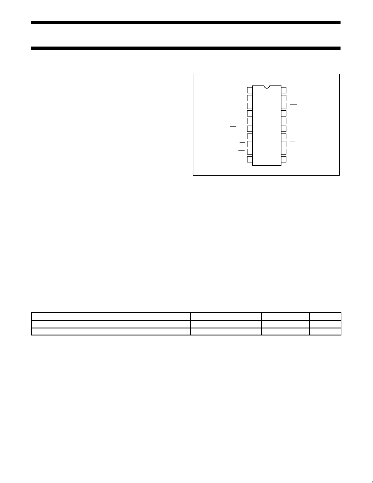
PIN CONFIGURATION
D, F, N Packages
VIN 1
DB0 2
DB1 3
DB2 4
DB3 5
WR/RDY 6
MODE 7
RD 8
INT 9
GND 10
20 VDD
19 NC
18 OFL
17 DB7
16 DB6
15 DB5
14 DB4
13 CS
12 VREF(+)
11 VREF(–)
TOP VIEW
APPLICATIONS
• Microprocessor-based monitoring and control systems
• Transducer/µP interface
• Process control
• Logic analyzers
• Test and measurement
TEMPERATURE RANGE
0 to +70°C
0 to +70°C
ORDER CODE
ADC0820CNEN
ADC0820CNED
DWG #
0408B
1021B
August 31, 1994
568 853-1631 13721
1 page 
Philips Semiconductors Linear Products
8-Bit, high-speed, µP-compatible A/D converter with
track/hold function
Product specification
ADC0820
AC ELECTRICAL CHARACTERISTICS
VDD = 5V, tR = tF = 20ns, VREF(+) = 5V, VREF(-) = 0V, and TA = 25°C, unless otherwise specified.
SYMBOL
PARAMETER
TEST CONDITIONS
Min
tCRD
tACCO
Conversion time for RD mode
Access time (delay from falling edge of
RD to output valid)
Mode=0, Figure 1
Mode=0, Figure 1
tCWR-RD Conversion time for WR-RD mode
Mode=VDD, tWR=600ns, tRD=600ns;
Figures 3a and 3b
tWR
tRD
tACC1
tACC2
Write time
Read time
Min
Max
Min
Access time (delay from falling edge of
RD t o output valid)
Access time (delay from falling edge of
RD t o output valid)
tI
t1H, t0H
Internal comparison time
Three-state control (delay from rising
edge of RD to Hi-Z state)
Mode=VDD, Figures 3a and 3b2
Mode=VDD, Figures 3a and 3b2
Mode=VDD, tRD<tI;
Figure 3b, CL=15pF
CL=100pF
Mode=VDD, tRD>tI;
Figure 3a, CL=15pF
CL=100pF
Mode=VDD;
Figures 2 and 3a, CL=50pF
RL=1kΩ, CL=10pF
600
600
tINTL
tINTH
tINTHWR
Delay from rising edge of WR to falling
edge of INT
Delay from rising edge of RD to rising
edge of INT
Delay from rising edge of WR to rising
edge of INT
Mode=VDD, CL=50pF
tRD>tI; Figure 3a
tRD<tI; Figure 3b
Figures 1, 3a, and 3b,
CL=50pF
Figure 2, CL=50pF
tRDY
tID
tRI
Delay from CS to RDY
Delay from INT to output valid
Delay from RD to INT
Figure 1, CL=50pF, Mode=0
Figure 2
Mode=VDD, tRD<tI;
Figure 3b
tP
Delay from end of conversion to next
conversion
Figures 1, 2, 3a, and 3b2
500
SR Slew rate, tracking
CVIN
Analog input capacitance
COUT
Logic output capacitance
CIN Logic input capacitance
NOTES:
1. Unadjusted error includes offset, full-scale, and linearity errors.
2. Accuracy may degrade if tWR or tRD is shorter than the minimum value specified.
3. Typical values are at 25°C and represent most likely parametric norm.
4. Guaranteed but not 100% production tested. These limits are not used to calculate outgoing quality levels.
5. VREF and VIN must be applied after VCC has been turned on to prevent possibility of latching.
LIMITS4
Typ3
1.6
Max
2.5
tCRD+20 tCRD+50
UNIT
µs
ns
1.52 µs
ns
50 µs
ns
190 280
ns
210 320
70 120 ns
90 150 ns
800 1300 ns
100 200 ns
tRD+200
125
tI
tRD+290
225
ns
ns
ns
175 270 ns
50 100 ns
20 50 ns
200 290 ns
ns
0.1 V/µs
45 pF
5 pF
5 pF
August 31, 1994
572
5 Page 
Philips Semiconductors Linear Products
8-Bit, high-speed, µP-compatible A/D converter with
track/hold function
Product specification
ADC0820
WR
• MS COMPARATORS ZERO
TO REFERENCE LADDER.
• LS COMPARATORS FLOAT
600ns
• MS COMPARATORS COMPARE
VIN TO THEIR REFERENCE
LADDER TAP. THE COMPARATOR
VIN • VLADDER TAP.
• LS COMPARATORS ZERO TO VIN
THE COMPARATOR’S INPUT
CAPACTORS TRACK VIN.
• MS COMPARATORS OUT–
PUTS ARE LATCHED. THE
MS DAC IS SET. THE MS
COMPARATOR FLOATS.
• LS COMPARATORS COM–
PARE LSB SECTION OF REF–
ERENCE LADDER
Figure 8. Operating Sequence (WR-RD Mode)
• LS COMPARATORS OUTPUTS
ARE LATCHED AND
CAN BE READ
• MS COMPARATORS RE
TURN TO ZERO MODE.
VIN(+)
VIN(–)
1.2k
5V
IN+
GND
REF (+)
2.5V
REF(–)
VIN(+)
VIN(–)
5V
IN+
GND
REF (+)
REF(–)
a. External Reference 2.5V Full-Scale
b. Power Supply as Reference
Figure 9. Analog Input Options
VIN(+)
IN+
1.2k
5V
2.5V
VIN(–)
GND
REF (+)
REF(–)
• CURRENT PATH MUST
STILL EXIST FROM
VIN(–) TO GROUND
c. Input not Referred to GND
August 31, 1994
578
11 Page | ||
| Páginas | Total 14 Páginas | |
| PDF Descargar | [ Datasheet ADC0820CNEN.PDF ] | |
Hoja de datos destacado
| Número de pieza | Descripción | Fabricantes |
| ADC0820CNED | 8-Bit/ high-speed/ mP-compatible A/D converter with track/hold function | NXP Semiconductors |
| ADC0820CNEN | 8-Bit/ high-speed/ mP-compatible A/D converter with track/hold function | NXP Semiconductors |
| Número de pieza | Descripción | Fabricantes |
| SLA6805M | High Voltage 3 phase Motor Driver IC. |
Sanken |
| SDC1742 | 12- and 14-Bit Hybrid Synchro / Resolver-to-Digital Converters. |
Analog Devices |
|
DataSheet.es es una pagina web que funciona como un repositorio de manuales o hoja de datos de muchos de los productos más populares, |
| DataSheet.es | 2020 | Privacy Policy | Contacto | Buscar |