|
|
|
PDF ADC0820 Data sheet ( Hoja de datos )
| Número de pieza | ADC0820 | |
| Descripción | 8-Bit High Speed P Compatible A/D Converter with Track/Hold Function | |
| Fabricantes | National Semiconductor | |
| Logotipo | ||
Hay una vista previa y un enlace de descarga de ADC0820 (archivo pdf) en la parte inferior de esta página. Total 22 Páginas | ||
|
No Preview Available !
June 1999
ADC0820
8-Bit High Speed µP Compatible A/D Converter with
Track/Hold Function
General Description
By using a half-flash conversion technique, the 8-bit
ADC0820 CMOS A/D offers a 1.5 µs conversion time and
dissipates only 75 mW of power. The half-flash technique
consists of 32 comparators, a most significant 4-bit ADC and
a least significant 4-bit ADC.
The input to the ADC0820 is tracked and held by the input
sampling circuitry eliminating the need for an external
sample-and-hold for signals moving at less than 100 mV/µs.
For ease of interface to microprocessors, the ADC0820 has
been designed to appear as a memory location or I/O port
without the need for external interfacing logic.
Key Specifications
n Resolution
n Conversion Time
n Low Power
n Total Unadjusted
Error
8 Bits
2.5 µs Max (RD Mode)
1.5 µs Max (WR-RD Mode)
75 mW Max
±1⁄2 LSB and ± 1 LSB
Features
n Built-in track-and-hold function
n No missing codes
n No external clocking
n Single supply — 5 VDC
n Easy interface to all microprocessors, or operates
stand-alone
n Latched TRI-STATE® output
n Logic inputs and outputs meet both MOS and T2L
voltage level specifications
n Operates ratiometrically or with any reference value
equal to or less than VCC
n 0V to 5V analog input voltage range with single 5V
supply
n No zero or full-scale adjust required
n Overflow output available for cascading
n 0.3" standard width 20-pin DIP
n 20-pin molded chip carrier package
n 20-pin small outline package
n 20-pin shrink small outline package (SSOP)
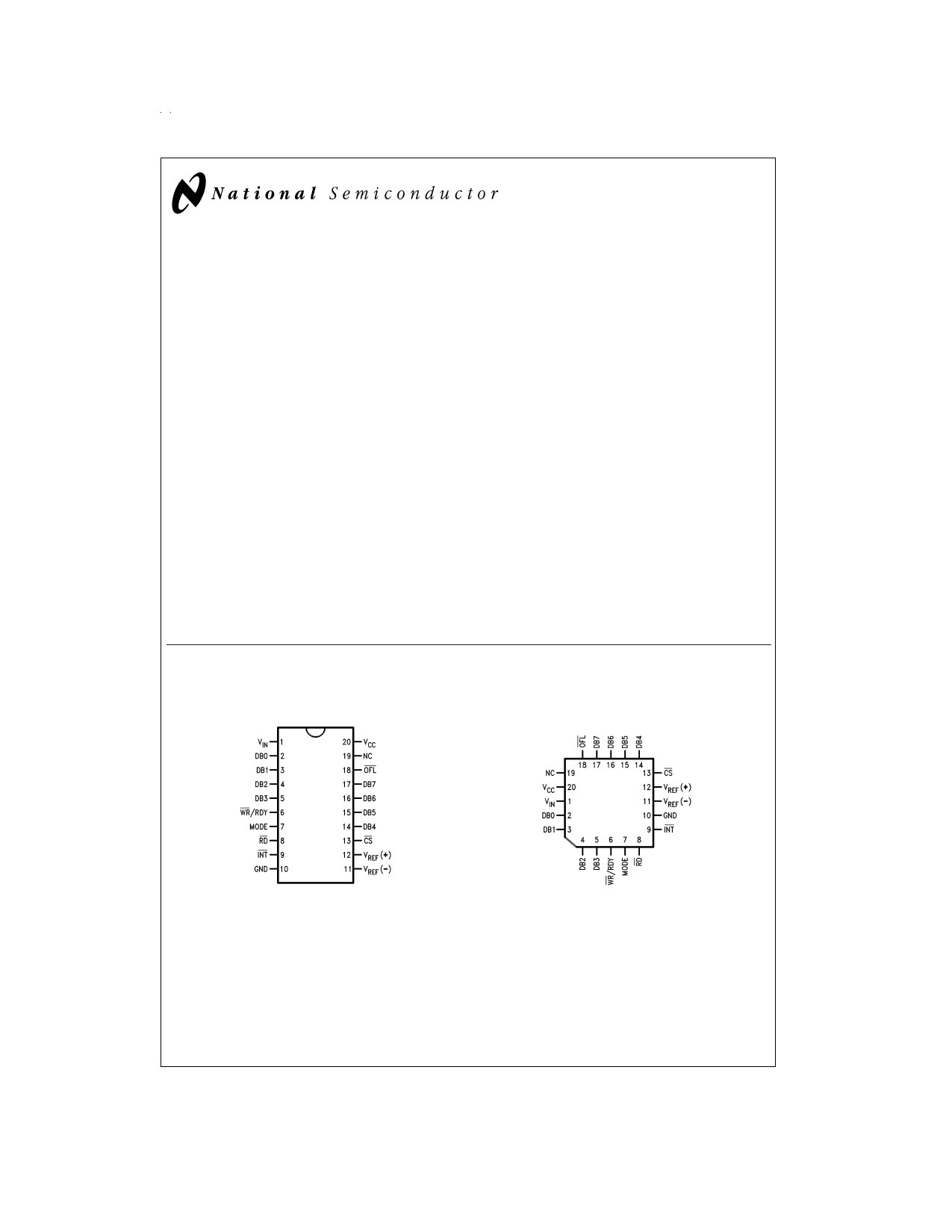
Connection and Functional Diagrams
Dual-In-Line, Small Outline
and SSOP Packages
Molded Chip Carrier
Package
Top View
DS005501-1
TRI-STATE® is a registered trademark of National Semiconductor Corporation.
© 1999 National Semiconductor Corporation DS005501
DS005501-33
www.national.com
1 page 
AC Electrical Characteristics (Continued)
The following specifications apply for VCC=5V, tr=tf=20 ns, VREF(+)=5V, VREF(−)=0V and TA=25˚C unless otherwise speci-
fied.
Typ
Tested
Design
Parameter
Conditions
(Note 6)
Limit
Limit
Units
tACC2, Access Time (Delay from
Falling Edge of RD to Output
Valid)
tACC3, Access Time (Delay from
Rising Edge of RDY to Output
Valid)
tI, Internal Comparison Time
t1H, t0H, TRI-STATE Control
(Delay from Rising Edge of RD to
Pin 7 = VCC, tRD>tI; Figure 4
CL=15 pF
CL=100 pF
RPULLUP = 1k and CL = 15 pF
Pin 7=VCC; Figures 4, 5
CL=50 pF
RL=1k, CL=10 pF
(Note 7)
(Note 8)
70 120 ns
90 150 ns
30 ns
800
1300
ns
100 200 ns
Hi-Z State)
tINTL, Delay from Rising Edge of
WR to Falling Edge of INT
tINTH, Delay from Rising Edge of
RD to Rising Edge of INT
tINTHWR, Delay from Rising Edge of
WR to Rising Edge of INT
tRDY, Delay from CS to RDY
tID, Delay from INT to Output Valid
tRI, Delay from RD to INT
Pin 7 = VCC, CL= 50 pF
tRD>tI; Figure 4
tRD<tI; Figure 3
Figures 2, 3, 4
CL=50 pFc
Figure 5, CL=50 pF
Figure 2, CL=50 pF, Pin 7 =0
Figure 5
Pin 7=VCC, tRD<tI
Figure 3
tRD+200
125
175
50
20
200
tI
tRD+290
225
270
100
50
290
ns
ns
ns
ns
ns
ns
ns
tP, Delay from End of Conversion
to Next Conversion
Figures 2, 3, 4, 5
(Note 4) See Graph
500 ns
Slew Rate, Tracking
0.1 V/µs
CVIN, Analog Input Capacitance
COUT, Logic Output Capacitance
CIN, Logic Input Capacitance
45 pF
5 pF
5 pF
Note 1: Absolute Maximum Ratings indicate limits beyond which damage to the device may occur. DC and AC electrical specifications do not apply when operating
the device beyond its specified operating conditions.
Note 2: All voltages are measured with respect to the GND pin, unless otherwise specified.
Note 3: Total unadjusted error includes offset, full-scale, and linearity errors.
Note 4: Accuracy may degrade if tWR or tRD is shorter than the minimum value specified. See Accuracy vs tWR and Accuracy vs tRD graphs.
Note 5: When the input voltage (VIN) at any pin exceeds the power supply rails (VIN < V−or VIN > V+) the absolute value of current at that pin should be limited to
1 mA or less. The 4 mA package input current limits the number of pins that can exceed the power supply boundaries with a 1 mA current limit to four.
Note 6: Typicals are at 25˚C and represent most likely parametric norm.
Note 7: Tested limits are guaranteed to National’s AOQL (Average Outgoing Quality Level).
Note 8: Design limits are guaranteed but not 100% tested. These limits are not used to calculate outgoing quality levels.
Note 9: Human body model, 100 pF discharaged through a 1.5 kΩ resistor.
5 www.national.com
5 Page 
1.0 Functional Description (Continued)
sured while WR is low. In RD mode, sampling occurs during
the first 800 ns of RD. Because of the input connections to
the ADC0820’s LS and MS comparators, the converter has
the ability to sample VIN at one instant (Section 2.4), despite
the fact that two separate 4-bit conversions are being done.
More specifically, when WR is low the MS flash is in compare
mode (connected to VIN), and the LS flash is in zero mode
(also connected to VIN). Therefore both flash ADCs sample
VIN at the same time.
1.4 DIGITAL INTERFACE
The ADC0820 has two basic interface modes which are se-
lected by strapping the MODE pin high or low.
RD Mode
With the MODE pin grounded, the converter is set to Read
mode. In this configuration, a complete conversion is done
by pulling RD low until output data appears. An INT line is
provided which goes low at the end of the conversion as well
as a RDY output which can be used to signal a processor
that the converter is busy or can also serve as a system
Transfer Acknowledge signal.
RD Mode (Pin 7 is Low)
conversion time is desired, the processor need not wait for
INT and can exercise a read after only 600 ns (Figure 9 ). If
this is done, INT will immediately go low and data will appear
at the outputs.
DS005501-17
FIGURE 9. WR-RD Mode (Pin 7 is High and tRD<tI)
DS005501-16
When in RD mode, the comparator phases are internally trig-
gered. At the falling edge of RD, the MS flash converter goes
from zero to compare mode and the LS ADC’s comparators
enter their zero cycle. After 800 ns, data from the MS flash is
latched and the LS flash ADC enters compare mode. Follow-
ing another 800 ns, the lower 4 bits are recovered.
WR then RD Mode
With the MODE pin tied high, the A/D will be set up for the
WR-RD mode. Here, a conversion is started with the WR in-
put; however, there are two options for reading the output
data which relate to interface timing. If an interrupt driven
scheme is desired, the user can wait for INT to go low before
reading the conversion result (Figure 10 ). INT will typically
go low 800 ns after WR’s rising edge. However, if a shorter
DS005501-18
FIGURE 10. WR-RD Mode (Pin 7 is High and tRD>tI)
Stand-Alone
For stand-alone operation in WR-RD mode, CS and RD can
be tied low and a conversion can be started with WR. Data
will be valid approximately 800 ns following WR’s rising
edge.
WR-RD Mode (Pin 7 is High) Stand-Alone Operation
DS005501-19
11 www.national.com
11 Page | ||
| Páginas | Total 22 Páginas | |
| PDF Descargar | [ Datasheet ADC0820.PDF ] | |
Hoja de datos destacado
| Número de pieza | Descripción | Fabricantes |
| ADC0820 | 8-Bit High Speed P Compatible A/D Converter with Track/Hold Function | National Semiconductor |
| ADC0820 | 8-Bit/ high-speed/ mP-compatible A/D converter with track/hold function | NXP Semiconductors |
| ADC0820 | CMOS High Speed 8-Bit A/D Converter with Track/Hold Function | Maxim Integrated Products |
| ADC0820-N | ADC0820 8-Bit High Speed uP Compatible A/D Converter with Track/Hold Function (Rev. C) | Texas Instruments |
| Número de pieza | Descripción | Fabricantes |
| SLA6805M | High Voltage 3 phase Motor Driver IC. |
Sanken |
| SDC1742 | 12- and 14-Bit Hybrid Synchro / Resolver-to-Digital Converters. |
Analog Devices |
|
DataSheet.es es una pagina web que funciona como un repositorio de manuales o hoja de datos de muchos de los productos más populares, |
| DataSheet.es | 2020 | Privacy Policy | Contacto | Buscar |