|
|
|
PDF AD9852 Data sheet ( Hoja de datos )
| Número de pieza | AD9852 | |
| Descripción | CMOS 300 MHz Complete-DDS | |
| Fabricantes | Analog Devices | |
| Logotipo | ||
Hay una vista previa y un enlace de descarga de AD9852 (archivo pdf) en la parte inferior de esta página. Total 30 Páginas | ||
|
No Preview Available !
FEATURES
300 MHz internal clock rate
FSK, BPSK, PSK, chirp, AM operation
Dual integrated 12-bit D/A converters
Ultrahigh speed comparator, 3 ps rms jitter
Excellent dynamic performance
80 dB SFDR at 100 MHz (±1 MHz) AOUT
4× to 20× programmable reference clock multiplier
Dual 48-bit programmable frequency registers
Dual 14-bit programmable phase offset registers
12-bit programmable amplitude modulation and on/off
output shaped keying function
Single-pin FSK and BPSK data interfaces
PSK capability via I/O interface
Linear or nonlinear FM chirp functions with single pin
frequency hold function
CMOS 300 MSPS Complete DDS
AD9852
Frequency ramped FSK
<25 ps rms total jitter in clock generator mode
Automatic bidirectional frequency sweeping
Sin(x)/x correction
Simplified control interface
10 MHz serial 2-wire or 3-wire SPI-compatible
100 MHz parallel 8-bit programming
3.3 V single supply
Multiple power-down functions
Single-ended or differential input reference clock
Small, 80-lead LQFP or TQFP with exposed pad
APPLICATIONS
Agile LO frequency synthesis
Programmable clock generator
FM chirp source for radar and scanning systems
Test and measurement equipment
Commercial and amateur RF exciter
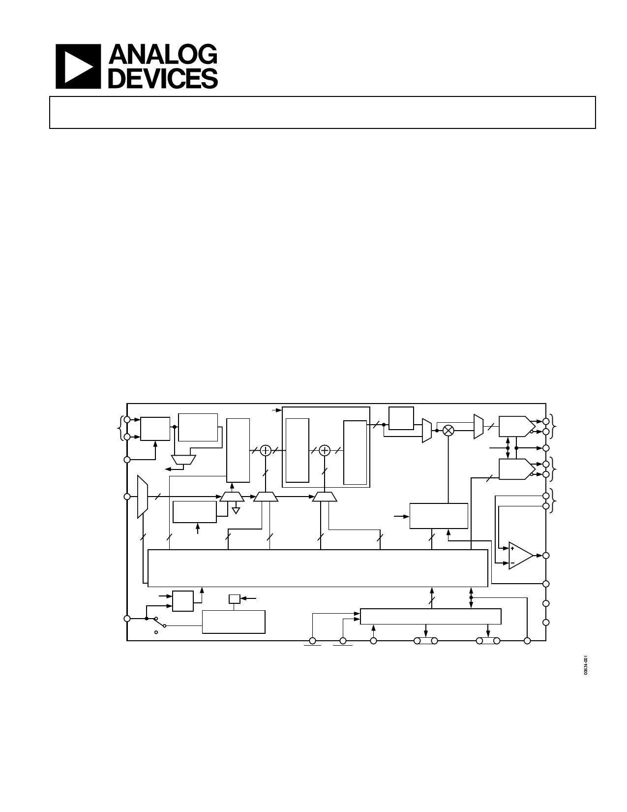
FUNCTIONAL BLOCK DIAGRAM
REFERENCE
CLOCK IN
DIFF/SINGLE
SELECT
FSK/BPSK/HOLD
DATA IN
REFCLK
BUFFER
SYSTEM CLOCK
4× TO 20×
REFCLK
MULTIPLIER
48 48
SYSTEM
CLOCK
MUX
3
MUX
DELTA
FREQUENCY
RATE TIMER
48
MUX
DDS CORE
17 17
14
MUX
12
I
Q
INV
SINC
FILTER
DIGITAL MULTIPLIERS
12
12-BIT
COSINE
DAC
SYSTEM
CLOCK
12-BIT
CONTROL
DAC
12
SYSTEM
CLOCK
PROGRAMMABLE
AMPLITUDE AND
RATE CONTROL
ANALOG
OUT
DAC RSET
ANALOG
OUT
ANALOG
IN
2
48 SYSTEM
48
CLOCK
48
DELTA
FREQUENCY
WORD
FREQUENCY FREQUENCY
TUNING
TUNING
WORD 1
WORD 2
14
FIRST 14-BIT
PHASE/OFFSET
WORD
14 12
SECOND 14-BIT
AM 12-BIT DC
PHASE/OFFSET MODULATION CONTROL
WORD
COMPARATOR
CLOCK
OUT
BIDIRECTIONAL
INTERNAL/EXTERNAL
I/O UPDATE CLOCK
MODE SELECT
SYSTEM
CLOCK
INT
CLK
DQ
EXT
PROGRAMMING REGISTERS
SYSTEM
÷2 CLOCK
AD9852
INTERNAL
PROGRAMMABLE
UPDATE CLOCK
BUS
I/O PORT BUFFERS
OSK
GND
+VS
READ
WRITE SERIAL/
PARALLEL
SELECT
Figure 1.
6-BIT ADDRESS
OR SERIAL
PROGRAMMING
LINES
8-BIT
PARALLEL
LOAD
MASTER
RESET
Rev. E
Information furnished by Analog Devices is believed to be accurate and reliable. However, no
responsibility is assumed by Analog Devices for its use, nor for any infringements of patents or other
rights of third parties that may result from its use. Specifications subject to change without notice. No
license is granted by implication or otherwise under any patent or patent rights of Analog Devices.
Trademarksandregisteredtrademarksarethepropertyoftheirrespectiveowners.
One Technology Way, P.O. Box 9106, Norwood, MA 02062-9106, U.S.A.
Tel: 781.329.4700
www.analog.com
Fax: 781.461.3113 ©2002–2007 Analog Devices, Inc. All rights reserved.
1 page 
REVISION HISTORY
5/07—Rev. D to Rev. E
Changed AD9852ASQ to AD9852ASVZ ....................... Universal
Changed AD9852AST to AD9852ASTZ......................... Universal
Change to Features............................................................................1
Changes to Endnote 10 of Table 1...................................................7
Changes to Absolute Maximum Ratings........................................8
Added Thermal Resistance Section ................................................8
Change to Ramped FSK (Mode 010) Section..............................19
Change to Internal and External Update Clock Section............27
Change to Thermal Impedance Section.......................................38
Changes to Junction Temperature Considerations Section.......38
Changes to Thermally Enhanced Package Mounting
Guidelines Section......................................................................40
Deleted Figure 61 to Figure 64 ......................................................41
Changes to Table 14 ........................................................................44
Updated Outline Dimensions........................................................51
Changes to Ordering Guide...........................................................52
12/05—Rev. C to Rev. D
Updated Format.................................................................. Universal
Changes to General Description .....................................................4
Changes to Explanation of Test Levels Section .............................9
Change to Pin Configuration ........................................................10
Changes to Figure 65 ......................................................................47
Changes to Outline Dimensions ...................................................52
Changes to Ordering Guide...........................................................52
4/04—Rev. B to Rev. C
Updated Format.................................................................. Universal
Changes to Figure 1...........................................................................1
Changes to General Description .....................................................3
Changes to Table 1 ............................................................................4
Changes to Footnote 2 ......................................................................6
Changes to Figure 2...........................................................................8
Changes to Table 5 ..........................................................................17
Changes to Equation in Ramped FSK (Mode 010).....................19
Changes to Evaluation Board Instructions ..................................39
Changes to General Operating Instructions Section..................39
Changes to Using the Provided Software Section.......................42
Changes to Figure 65 ......................................................................43
Changes to Figure 66 ......................................................................44
Changes to Figure 72 and Figure 73 .............................................48
Changes to Ordering Guide...........................................................48
AD9852
3/02—Rev. A to Rev. B
Changes to General Description .....................................................1
Changes to Functional Block Diagram ..........................................1
Changes to Specifications ................................................................3
Changes to Absolute Maximum Ratings........................................5
Changes to Pin Function Descriptions ..........................................6
Changes to Figure 3 ..........................................................................8
Deleted Two TPCs ..........................................................................11
Changes to Figure 18 and Figure 19 .............................................11
Changes to BPDK Mode Section ..................................................21
Changes to Differential Refclk Enable Section ...........................24
Changes to Master Reset Section ..................................................24
Changes to Parallel I/O Operation Section .................................24
Changes to General Operation of the Serial
Interface Section..............................................................................27
Changes to Figure 50 ......................................................................27
Changes to Figure 65 ......................................................................36
Rev. E | Page 3 of 52
5 Page 
PIN CONFIGURATION AND FUNCTION DESCRIPTIONS
AD9852
80 79 78 77 76 75 74 73 72 71 70 69 68 67 66 65 64 63 62 61
D7 1
D6 2
D5 3
D4 4
D3 5
D2 6
D1 7
D0 8
DVDD 9
DVDD 10
DGND 11
DGND 12
NC 13
A5 14
A4 15
A3 16
A2/IO RESET 17
A1/SDO 18
A0/SDIO 19
I/O UD CLK 20
PIN 1
AD9852
TOP VIEW
(Not to Scale)
21 22 23 24 25 26 27 28 29 30 31 32 33 34 35 36 37 38 39 40
NC = NO CONNECT
60 AVDD
59 AGND
58 NC
57 NC
56 DAC RSET
55 DACBP
54 AVDD
53 AGND
52 IOUT2
51 IOUT2
50 AVDD
49 IOUT1
48 IOUT1
47 AGND
46 AGND
45 AGND
44 AVDD
43 VINN
42 VINP
41 AGND
Figure 2. Pin Configuration
Table 5. Pin Function Descriptions
Pin Number
Mnemonic
1 to 8
D7 to D0
9, 10, 23, 24, 25,
73, 74, 79, 80
DVDD
11, 12, 26, 27, 28,
72, 75 to 78
DGND
13, 35, 57, 58, 63
NC
14 to 16
A5 to A3
17 A2/IO RESET
18 A1/SDO
Description
8-Bit Bidirectional Parallel Programming Data Inputs. Used only in parallel programming mode.
Connections for the Digital Circuitry Supply Voltage. Nominally 3.3 V more positive than AGND
and DGND.
Connections for Digital Circuitry Ground Return. Same potential as AGND.
No Internal Connection.
Parallel Address Inputs for Program Registers (Part of 6-Bit Parallel Address Inputs for Program
Register, A5:A0). Used only in parallel programming mode.
Parallel Address Input for Program Registers (Part of 6-Bit Parallel Address Inputs for Program
Register, A5:A0)/IO Reset. A2 is used only in parallel programming mode. IO RESET is used when
the serial programming mode is selected, allowing an IO RESET of the serial communication bus
that is unresponsive due to improper programming protocol. Resetting the serial bus in this
manner does not affect previous programming, nor does it invoke the default programming
values seen in Table 9. Active high.
Parallel Address Input for Program Registers (Part of 6-Bit Parallel Address Inputs for Program
Register, A5:A0)/Unidirectional Serial Data Output. A1 is used only in parallel programming
mode. SDO is used in 3-wire serial communication mode when the serial programming mode is
selected.
Rev. E | Page 9 of 52
11 Page | ||
| Páginas | Total 30 Páginas | |
| PDF Descargar | [ Datasheet AD9852.PDF ] | |
Hoja de datos destacado
| Número de pieza | Descripción | Fabricantes |
| AD9850 | 125 MHz Complete DDS Synthesizer | Analog Devices |
| AD9851 | CMOS 180 MHz DDS/DAC Synthesizer | Analog Devices |
| AD9852 | CMOS 300 MHz Complete-DDS | Analog Devices |
| AD9853 | Programmable Digital OPSK/16-QAM Modulator | Analog Devices |
| Número de pieza | Descripción | Fabricantes |
| SLA6805M | High Voltage 3 phase Motor Driver IC. |
Sanken |
| SDC1742 | 12- and 14-Bit Hybrid Synchro / Resolver-to-Digital Converters. |
Analog Devices |
|
DataSheet.es es una pagina web que funciona como un repositorio de manuales o hoja de datos de muchos de los productos más populares, |
| DataSheet.es | 2020 | Privacy Policy | Contacto | Buscar |