|
|
|
PDF AD9821 Data sheet ( Hoja de datos )
| Número de pieza | AD9821 | |
| Descripción | Complete 12-Bit 40 MSPS Imaging Signal Processor | |
| Fabricantes | Analog Devices | |
| Logotipo | ||
Hay una vista previa y un enlace de descarga de AD9821 (archivo pdf) en la parte inferior de esta página. Total 16 Páginas | ||
|
No Preview Available !
FEATURES
Differential Sensor Input with 1 V p-p Input Range
0 dB to 36 dB 10-Bit Variable Gain Amplifier (VGA)
Low Noise Optical Black Clamp Circuit
Analog Preblanking Function
12-Bit 40 MSPS A/D Converter (ADC)
3-Wire Serial Digital Interface
3 V Single-Supply Operation
Low Power: 150 mW @ 3 V Supply
48-Lead LQFP Package
APPLICATIONS
Digital Still Cameras Using CMOS Imagers
Industrial/Scientific Imaging
Complete 12-Bit 40 MSPS
Imaging Signal Processor
AD9821
GENERAL DESCRIPTION
The AD9821 is a complete analog signal processor for imaging
applications that do not require Correlated Double Sampling
(CDS). It features a 40 MHz single-channel architecture designed
to sample and condition the outputs of CMOS imagers and CCD
arrays already containing on-chip CDS. The AD9821’s signal
chain consists of a differential input sample-and-hold amplifier
(SHA), digitally controlled variable gain amplifier (VGA), black
level clamp, and a 12-bit ADC.
The internal registers are programmed through a 3-wire serial
digital interface. Programmable features include gain adjust-
ment, black level adjustment, and power-down modes.
The AD9821 operates from a single 3 V power supply, typically
dissipates 150 mW, and is packaged in a 48-lead LQFP.
VIN+
VIN–
BYP1
FUNCTIONAL BLOCK DIAGRAM
AVDD AVSS
VRT VRB
AD9821
+
SHA
–
0dB ~ 36dB
VGA
BAND GAP
REFERENCE
12-BIT
ADC
PBLK
12
DRVDD
DRVSS
DOUT
10 CLP
INTERNAL
REGISTERS
DIGITAL
INTERFACE
8 BLK CLAMP
LEVEL
CLPOB
DVDD
DVSS
SL SCK SDATA
DATACLK
REV. 0
Information furnished by Analog Devices is believed to be accurate and
reliable. However, no responsibility is assumed by Analog Devices for its
use, nor for any infringements of patents or other rights of third parties that
may result from its use. No license is granted by implication or otherwise
under any patent or patent rights of Analog Devices.
One Technology Way, P.O. Box 9106, Norwood, MA 02062-9106, U.S.A.
Tel: 781/329-4700
www.analog.com
Fax: 781/326-8703
© Analog Devices, Inc., 2002
1 page 
PIN CONFIGURATION
48 47 46 45 44 43 42 41 40 39 38 37
(LSB) D0 1
D1 2
D2 3
D3 4
D4 5
D5 6
D6 7
D7 8
D8 9
D9 10
D10 11
(MSB) D11 12
PIN 1
IDENTIFIER
AD9821
TOP VIEW
(Not to Scale)
36 TEST
35 AVSS
34 TEST
33 AVDD2
32 BYP1
31 VIN–
30 VIN+
29 TEST
28 TEST
27 AVDD1
26 AVSS
25 AVSS
NC = NO CONNECT 13 14 15 16 17 18 19 20 21 22 23 24
AD9821
PIN FUNCTION DESCRIPTIONS
Pin Number
Mnemonic
Type
Description
1–12
13
14
15, 41
16
17
18, 24, 37, 42, 47, 48
19
20
21–23
25, 26, 35
27
28, 29
30
31
32
33
34, 36
38
39
40
43
44
45
46
D0–D11
DRVDD
DRVSS
DVSS
DATACLK
DVDD1
NC
PBLK
CLPOB
TEST
AVSS
AVDD1
TEST
VIN+
VIN–
BYP1
AVDD2
TEST
VRT
VRB
DVDD2
STBY
SL
SDATA
SCK
DO
P
P
P
DI
P
NC
DI
DI
DI
P
P
AO
AI
AI
AO
P
AI
AO
AO
P
DI
DI
DI
DI
Digital Data Outputs
Digital Output Driver Supply
Digital Output Driver Ground
Digital Ground
Digital Data Output Latch Clock
Digital Supply
Internally Not Connected. May be Tied High or Low.
Preblanking Clock Input
Black Level Clamp Clock Input
Test Use Only. Tie to VDD or VSS.
Analog Ground
Analog Supply
Test Use Only. Tie to VDD or VSS.
Positive Analog Input for Imager Signal
Negative Analog Input for Imager Signal
Internal Bias Level Decoupling
Analog Supply
Test Use Only. Tie to VDD or VSS.
ADC Top Reference Voltage Decoupling
ADC Bottom Reference Voltage Decoupling
Digital Supply
Standby Mode, Active High. Same as Total Power-Down Mode.
Serial Digital Interface Load Pulse
Serial Digital Interface Data
Serial Digital Interface Clock
TYPE: AI = Analog Input, AO = Analog Output, DI = Digital Input, DO = Digital Output, P = Power.
REV. 0
–5–
5 Page 
AD9821
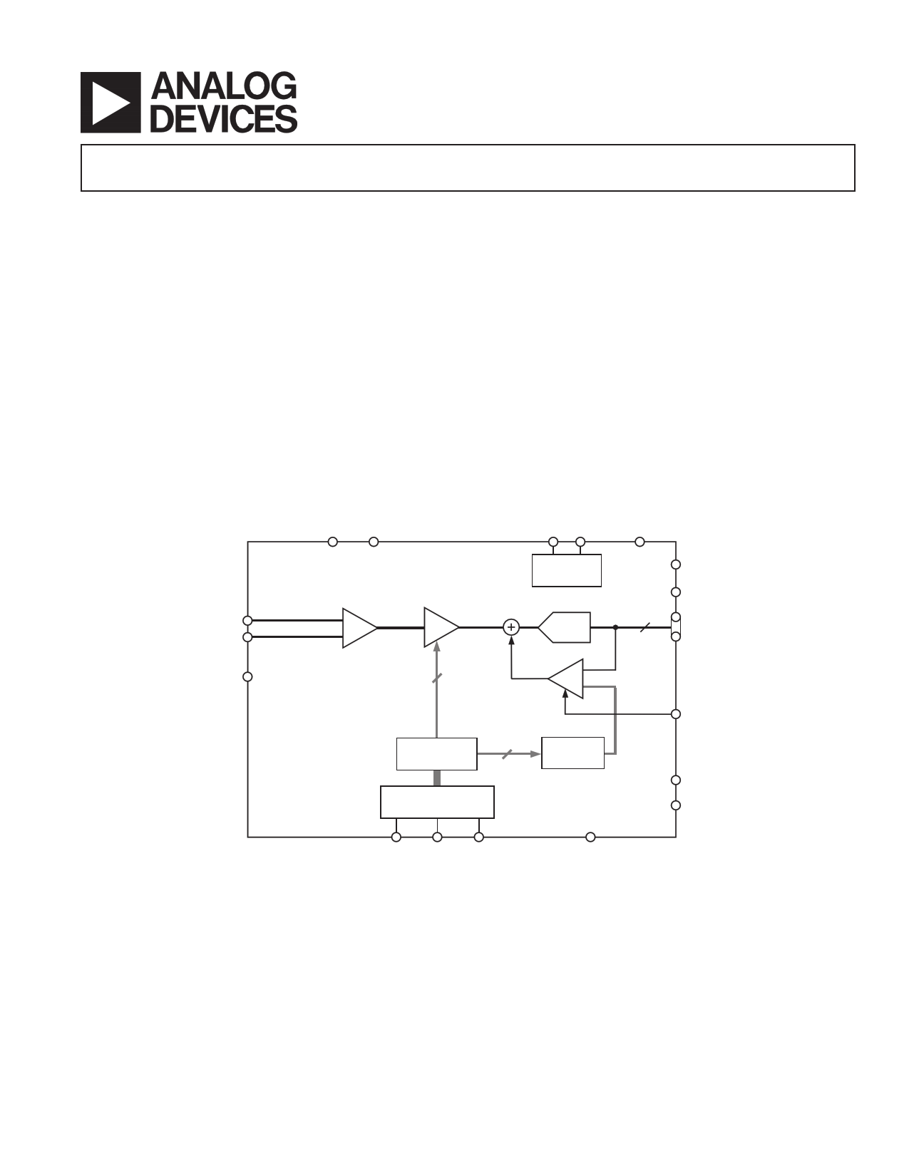
CIRCUIT DESCRIPTION AND OPERATION
The AD9821 signal processing chain is shown in Figure 10.
Each processing step is essential in achieving a high quality
image from the raw imager pixel data.
Differential Input SHA
The differential input SHA circuit is designed to accommodate
a variety of different image sensor output voltages. The timing
shown in Figure 8 illustrates how the DATACLK signal is used to
sample both the VIN+ and VIN– signals simultaneously. The
imager signal is sampled on the rising edges of DATACLK.
Placement of this clock signal is critical in achieving the best
performance from the imager. An internal DATACLK delay (tID)
of 3 ns is caused by internal propagation delays.
The differential input can be used in a variety of single-ended
and differential configurations, as shown in Table VI. The
allowable voltage range for both VIN+ or VIN– is from 0 V
to 1.8 V. Signal levels outside this range will result in severely
degraded performance. Regardless of the input configuration,
the voltage sampled by the SHA is always equal to VIN+ minus
VIN–. VIN+ must always be equal to or greater than VIN– or
negative clipping will occur. A small amount of offset between
the VIN+ and VIN– signals is allowable and can be corrected by
the Optical Black Clamp, up to ± 30 mV.
Note that the VIN+ and VIN– inputs do not contain any dc
restoration or bias circuitry. Therefore, dc-coupling is recom-
mended when driving the AD9821 analog inputs. If ac-coupling is
used, external biasing circuitry must be provided for the VIN+
and VIN– inputs to keep them in the acceptable common-mode
voltage range of 0 V to 1.8 V.
Table VI. Example Input Voltage Configurations
VIN+ Range (V) VIN– Range (V) SHA Output Range (V)
Black White Black White Black White
0 1.0
0.5 1.5
1.0 1.5
0.5 1.0
1.0 1.0
00
0 1.0
0.5 0.5 0 1.0
1.0 0.5 0 1.0
0.5 0
0 1.0
1.0 0
0 1.0
DATACLK
VIN+
VIN–
SHA
0dB TO 36dB
VGA
1.0F 1.0F
REFB
1.0V
REFT
2.0V
INTERNAL
VREF
12-BIT
ADC
12
BYP1
0.1F
0.45V
INTERNAL
BIAS
10
VGA GAIN
REGISTER
8-BIT
DAC
OPTICAL BLACK
CLAMP
DIGITAL
FILTERING
8
CLAMP LEVEL
REGISTER
Figure 10. Internal Block Diagram
PBLK
DOUT
CLPOB
REV. 0
–11–
11 Page | ||
| Páginas | Total 16 Páginas | |
| PDF Descargar | [ Datasheet AD9821.PDF ] | |
Hoja de datos destacado
| Número de pieza | Descripción | Fabricantes |
| AD9821 | Complete 12-Bit 40 MSPS Imaging Signal Processor | Analog Devices |
| AD9822 | Complete 14-Bit CCD/CIS Signal Processor | Analog Devices |
| AD9823 | Correlated Double Sampler (CDS) | Analog Devices |
| AD9824 | Complete 14-Bit 30 MSPS CCD Signal Processor | Analog Devices |
| Número de pieza | Descripción | Fabricantes |
| SLA6805M | High Voltage 3 phase Motor Driver IC. |
Sanken |
| SDC1742 | 12- and 14-Bit Hybrid Synchro / Resolver-to-Digital Converters. |
Analog Devices |
|
DataSheet.es es una pagina web que funciona como un repositorio de manuales o hoja de datos de muchos de los productos más populares, |
| DataSheet.es | 2020 | Privacy Policy | Contacto | Buscar |