|
|
|
PDF AD9807 Data sheet ( Hoja de datos )
| Número de pieza | AD9807 | |
| Descripción | Complete 12-Bit/10-Bit 6 MSPS CCD/CIS Signal Processors | |
| Fabricantes | Analog Devices | |
| Logotipo | ||
Hay una vista previa y un enlace de descarga de AD9807 (archivo pdf) en la parte inferior de esta página. Total 24 Páginas | ||
|
No Preview Available !
a
FEATURES
Pin Compatible 12-Bit and 10-Bit Versions
12-Bit/10-Bit 6 MSPS A/D Converter
Integrated Triple Correlated Double Sampler
3-Channel, 2 MSPS Color Mode
1؋ – 4؋ Analog Programmable Gain Amplifier
Pixel-Rate Digital Gain Adjustment
Pixel-Rate Digital Offset Adjustment
Internal Voltage Reference
No Missing Codes Guaranteed
Microprocessor-Compatible Control Interface
+3.3 V/+5 V Digital I/O Compatibility
Low Power CMOS: 500 mW
64-Pin PQFP Surface Mount Package
Complete 12-Bit/10-Bit 6 MSPS
CCD/CIS Signal Processors
AD9807/AD9805
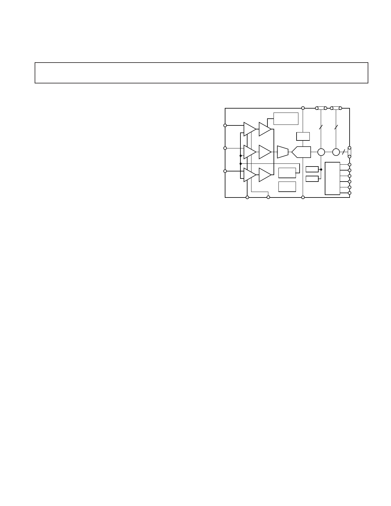
FUNCTIONAL BLOCK DIAGRAM
PIXEL PIXEL
VREF OFFSET GAIN
AD9807/AD9805
RED
VINR
CDS
PGA
GAIN
REGISTERS
8-10 12-10
REF
GREEN
VING
CDS
PGA
MUX
ADC
12-10
–X
DOUT
BLUE
VINB
CDS
PGA
INPUT
OFFSET
CONFIG
REGS
ODD
EVEN
MPU
PMOPRUT
PORT
CDSCLK1 CDSCLK2
ADCCLK
CSB
RD
WR
A2
A1
A0
PRODUCTION DESCRIPTION
The AD9807 and AD9805 are complete CCD/CIS imaging
decoders and signal processors on a single monolithic integrated
circuit. The input of the AD9807/AD9805 allows direct ac
coupling of the charge-coupled device (CCD) or contact image
sensor (CIS) output(s). The AD9807/AD9805 includes all the
circuitry to perform three-channel correlated double sampling
(CDS) and programmable gain adjustment of the CCD output;
a 12-bit or 10-bit analog-to-digital converter (ADC) quantizes
the analog signal. After digitization, the on-board digital signal
processor (DSP) circuitry allows pixel rate offset and gain correc-
tion. The DSP also corrects odd/even CCD register imbalance
errors. A parallel control bus provides a simple interface to
8-bit microcontrollers. The AD9807/AD9805 comes in a
space saving 64-pin plastic quad flatpack (PQFP) and is specified
over the commercial (0°C to +70°C) temperature range. By
disabling the CDS, the AD9807/AD9805 are also suitable for
non-CCD applications, or applications that do not require
CDS, such as CIS signal processing.
PRODUCT HIGHLIGHTS
The AD9807/AD9805 offers a complete, single chip CCD
imaging front end in a 64-pin plastic quad flatpack (PQFP).
On-Chip PGA—The AD9807/AD9805 includes a 3-channel
analog programmable gain amplifier; it is programmable from
1× to 4× in 16 increments.
On-Chip CDS—An integrated 3-channel correlated double
sampler allows easy ac coupling directly from the CCD sensor
outputs. Additionally, the CDS reduces low frequency noise
and reset feedthrough.
On-Chip Voltage Reference—The AD9807/AD9805 includes a
2 V bandgap reference that allows the input range of the device to
be configured for input spans up to 4 V.
6 MSPS A/D Converter—A highly linear 12-bit or 10-bit A/D
converter sequentially digitizes the red, green and blue CDS
outputs ensuring no missing code performance. The user may also
configure the AD9807/AD9805 for single channel operation.
Digital Gain & Offset Correction—Pixel rate digital gain and
offset correction blocks allow precise repeatable correction of
imaging system error sources.
Digital I/O Compatibility—The AD9807/AD9805 offers
+3.3 V/+5 V logic level compatibility.
Pin-Compatible 12-Bit and 10-Bit Versions—The AD9807 is
also offered in a pin-compatible 10-bit version, the AD9805,
allowing upgrade-ability and simplifying design issues across
different scanner models.
REV. 0
Information furnished by Analog Devices is believed to be accurate and
reliable. However, no responsibility is assumed by Analog Devices for its
use, nor for any infringements of patents or other rights of third parties
which may result from its use. No license is granted by implication or
otherwise under any patent or patent rights of Analog Devices.
One Technology Way, P.O. Box 9106, Norwood, MA 02062-9106, U.S.A.
Tel: 617/329-4700 World Wide Web Site: http://www.analog.com
Fax: 617/326-8703
© Analog Devices, Inc., 1997
1 page 
PIN CONFIGURATION
AD9807/AD9805
64 63 62 61 60 59 58 57 56 55 54 53 52 51 50 49
AVDD 1
AVSS 2
CAPT 3
CAPT 4
CAPB 5
CAPB 6
VREF 7
CML 8
VINR 9
AVSS 10
VING 11
AVSS 12
VINB 13
AVSS 14
AVDD 15
STRTLN 16
PIN 1
IDENTIFIER
AD9807
TOP VIEW
(Not to Scale)
48 A0
47 DOUT<11>
46 DOUT<10>
45 DOUT<9>
44 DOUT<8>
43 DOUT<7>/MPU<7>
42 DOUT<6>/MPU<6>
41 DRVDD
40 DRVSS
39 DOUT<5>/MPU<5>
38 DOUT<4>/MPU<4>
37 DOUT<3>/MPU<3>
36 DOUT<2>/MPU<2>
35 DOUT<1>/MPU<1>
34 DOUT<0>/MPU<0>
33 OEB
17 18 19 20 21 22 23 24 25 26 27 28 29 30 31 32
PIN DESCRIPTIONS
Pin No.
Pin Name
Type
Description
1, 15
2, 10, 12, 14
3, 4
5, 6
7
8
9
11
13
16
17
18
19
28, 52
29, 51
20
21–26
27
30
31
32
33
34
35–39, 42
40
41
43
44–46
47
48, 49, 50
53
54–63
64
AVDD
AVSS
CAPT
CAPB
VREF
CML
VINR
VING
VINB
STRTLN
CDSCLK1
CDSCLK2
ADCCLK
DVSS
DVDD
OFFSET<7>
OFFSET<6:1>
OFFSET<0>
CSB
RDB
WRB
OEB
DOUT<0>/MPU<0>
DOUT<1:6>/MPU<1:6>
DRVSS
DRVDD
DOUT<7>/MPU<7>
DOUT<8:10>
DOUT<11>
A0, A1, A2
GAIN<0>
GAIN<1:10>
GAIN<11>
P
P
AO
AO
AO
AO
AI
AI
AI
DI
DI
DI
DI
P
P
DI
DI
DI
DI
DI
DI
DI
DIO
DIO
P
P
DIO
DO
DO
DI
DI
DI
DI
+5 V Analog Supply.
Analog Ground.
Reference Decoupling. See Figure 22.
Reference Decoupling.
Internal Reference Output. Decouple with 10 µF + 0.1 µF.
Internal Bias Voltage. Decouple with 0.1 µF.
Analog Input, Red.
Analog Input, Green.
Analog Input, Blue.
STRTLN. Indicates beginning of scan line.
CDS Reset Clock Pulse Input.
CDS Data Clock Pulse Input.
A/D Sample Clock Input.
Digital Ground.
+5 V Digital Supply.
Pixel Rate Offset Coefficient Inputs. Most Significant Bit.
Pixel Rate Offset Coefficient Inputs.
Pixel Rate Offset Coefficient Inputs. Least Significant Bit.
Chip Select. Active Low.
Read Strobe. Active Low.
Write Strobe. Active Low.
Output Enable. Active Low.
Data Output LSB/Register Input LSB
Data Outputs/Register Inputs.
Digital Driver Ground
Digital Driver Supply
Data Output/Register Input MSB.
Data Outputs.
Data Output MSB.
Register Select Pins.
Pixel Rate Gain Coefficient Input. LSB.
Pixel Rate Gain Coefficient Inputs.
Pixel Rate Gain Coefficient Input. MSB.
TYPE: AI = Analog Input; AO = Analog Output; DI = Digital Input; DO = Digital Output; DIO = Digital Input/Output; P = Power.
REV. 0
–5–
5 Page 
RED
VINR
CDS
PGA
GREEN
VING
CDS
PGA
BLUE
VINB
CDS
PGA
AD9807/AD9805
AD9807/AD9805
VREF
OFFSET<M:0>
GAIN<N:0>
BANDGAP
REFERENCE
8-10
12-10/10-8
I/O
MUX
3
12-BIT/10-BIT
A/D
12 DIGITAL 12 DIGITAL
–X
SUBTRACTOR
MULTIPLIER
12
INPUT OFFSET
REGISTER
8
CONFIGURATION
REGISTER
R
G CONFIGURATION
B
REGISTER
2
R
RODD
REVEN
G GODD GEVEN
B
BODD
BEVEN
MPU
PORT
OEB
12
DOUT<11:0>/MPU<7:0>
CSB
RDB
WRB
A2
A1
A0
CDSCLK1 CDSCLK2 STRTLN ADCCLK
Figure 4. Block Diagram
REGISTER OVERVIEW
MPU Port Map
Table II shows the MPU Port Map. The MPU Port Map is
accessed through pins A0, A1 and A2 of the AD9807/AD9805,
and provides the decoding scheme for the various registers of
the AD9807/AD9805. When writing or reading from any of the
registers, the appropriate bits must be applied to A0–A2.
Table II. MPU Port Map Format
A2 A1 A0 Register
0 0 0 Configuration Register
0 0 1 Configuration Register 2
0 1 0 PGA Gain Register
0 1 1 Odd Offset Register
1 0 0 Even Offset Register
1 0 1 Input Offset Register
1 1 0 RESERVED
1 1 1 Bayer Mode
Configuration Register/AD9807
The Configuration Register controls three functions: a color
pointer, gain and offset pin configurations, and digital gain
scaling. Figure 5 shows the AD9807 Configuration Register.
Bits 0–2 control the digital scaling function. Setting a bit makes
the corresponding condition true. Resetting Bits 0–2 disables
and bypasses the digital multiplier. Bits 3–5 control the gain
and offset pin distribution. Resetting Bits 3–5 disables and
bypasses the digital subtracter and sets the gain word width to
12. Setting any bit makes the corresponding condition true. For
example, if Bit 3 is set, the 2 LSBs of the gain word become the
2 MSBs of the offset word. If Bit 4 is set, the LSB of the gain
word becomes MSB of the offset word. Bits 6 and 7 direct
register data written to the MPU<7:0> bus to the appropriate
red, green or blue register.
76 54 3 21 0
8X FULL SCALE
4X FULL SCALE
2X FULL SCALE
10-BIT GAIN, 10-BIT OFFSET
11-BIT GAIN, 9-BIT OFFSET
12-BIT GAIN, 8-BIT OFFSET
COLOR0
COLOR1
Figure 5. AD9807 Configuration Register Format
Configuration Register/AD9805
The Configuration Register controls three functions: a color
pointer, gain and offset pin configurations, and digital gain
scaling. Figure 6 shows the AD9805 Configuration Register.
Bits 0–2 control the digital scaling function. Setting a Bit
makes the corresponding condition true. Resetting Bits 0–2
disables and bypasses the digital multiplier. Bits 3–5 control
the gain and offset pin distribution. Resetting Bits 3–5 disables
and bypasses the digital subtracter and sets the gain word width
to 10. Setting any bit makes the corresponding condition true.
If Bit 3 is set, the 2 LSBs of the gain word become the 2 MSBs
of the offset word. If Bit 4 is set, the LSB of the gain word
becomes MSB of the offset word. Bits 6 and 7 direct register
data written to the MPU<7:0> bus to the appropriate red,
green or blue register.
76 54 3 21 0
8X FULL SCALE
4X FULL SCALE
2X FULL SCALE
8-BIT GAIN, 10-BIT OFFSET
9-BIT GAIN, 9-BIT OFFSET
10-BIT GAIN, 8-BIT OFFSET
COLOR0
COLOR1
REV. 0
Figure 6. AD9805 Configuration Register Format
–11–
11 Page | ||
| Páginas | Total 24 Páginas | |
| PDF Descargar | [ Datasheet AD9807.PDF ] | |
Hoja de datos destacado
| Número de pieza | Descripción | Fabricantes |
| AD9801 | CCD Signal Processor For Electronic Cameras | Analog Devices |
| AD9802 | CCD Signal Processor For Electronic Cameras | Analog Devices |
| AD9803 | CCD Signal Processor | Analog Devices |
| AD9804 | Complete 10-Bit 18 MSPS CCD Signal Processor | Analog Devices |
| Número de pieza | Descripción | Fabricantes |
| SLA6805M | High Voltage 3 phase Motor Driver IC. |
Sanken |
| SDC1742 | 12- and 14-Bit Hybrid Synchro / Resolver-to-Digital Converters. |
Analog Devices |
|
DataSheet.es es una pagina web que funciona como un repositorio de manuales o hoja de datos de muchos de los productos más populares, |
| DataSheet.es | 2020 | Privacy Policy | Contacto | Buscar |