|
|
|
PDF ACT-F512K32N-150P7C Data sheet ( Hoja de datos )
| Número de pieza | ACT-F512K32N-150P7C | |
| Descripción | ACT-F512K32 High Speed 16 Megabit FLASH Multichip Module | |
| Fabricantes | Aeroflex Circuit Technology | |
| Logotipo | ||
Hay una vista previa y un enlace de descarga de ACT-F512K32N-150P7C (archivo pdf) en la parte inferior de esta página. Total 20 Páginas | ||
|
No Preview Available !
ACT–F512K32 High Speed
16 Megabit FLASH Multichip Module
Features
CIRCUIT TECHNOLOGY
www.aeroflex.com
■ 4 Low Power 512K x 8 FLASH Die in One MCM
Package
■ TTL Compatible Inputs and CMOS Outputs
■ Access Times of 60, 70, 90, 120 and 150ns
■ +5V Programing, 5V ±10% Supply
■ 100,000 Erase/Program Cycles
■ Low Standby Current
■ Page Program Operation and Internal Program
Control Time
■ Sector Architecture (Each Die)
● 8 Equal size sectors of 64K bytes each
● Any Combination of Sectors can be erased with
one command sequence
● Supports full chip erase
■ Embedded Erase and Program Algorithms
■ MIL-PRF-38534 Compliant MCMs Available
■ Industry Standard Pinouts
■ Packaging – Hermetic Ceramic
● 68 Lead, .88" x .88" x .160" Single-Cavity Small
Outline gull wing, Aeroflex code# "F5" (Drops into
the 68 Lead JEDEC .99"SQ CQFJ footprint)
● 66 Pin, 1.08" x 1.08" x .160" PGA Type, No
Shoulder, Aeroflex code# "P3"
● 66 Pin, 1.08" x 1.08" x .185" PGA Type, With
Shoulder, Aeroflex code# "P7"
■ Internal Decoupling Capacitors for Low Noise
Operation
■ Commercial, Industrial and Military Temperature
Ranges
■ DESC SMD# 5962–94612
Released (P3,P7,F5)
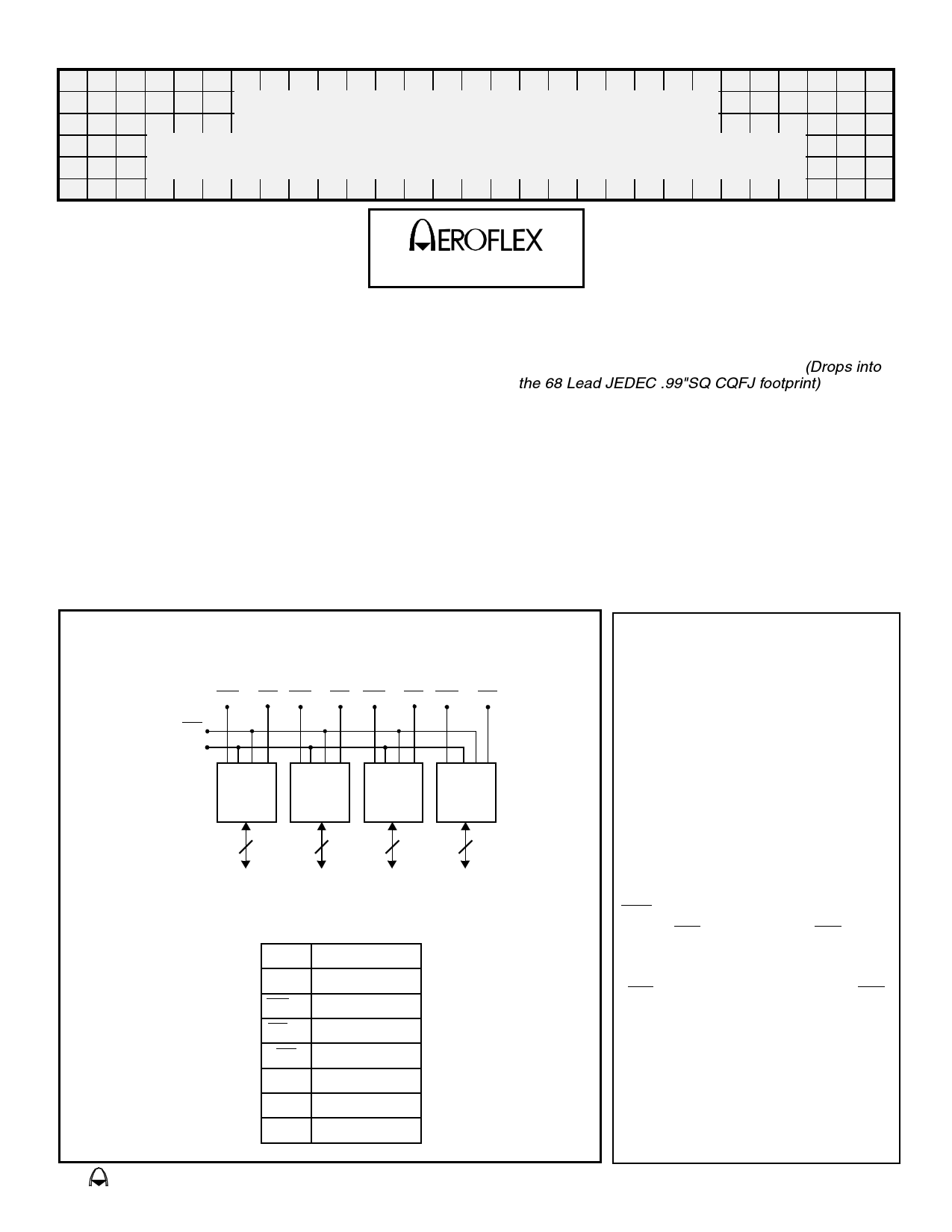
Block Diagram – PGA Type Package(P3,P7) & CQFP(F5)
WE1 CE1 WE2 CE2 WE3 CE3 WE4 CE4
OE
A0 – A18
512Kx8 512Kx8 512Kx8 512Kx8
8
I/O0-7
88 8
I/O8-15 I/O16-23 I/O24-31
Pin Description
I/O0-31 Data I/O
A0–18 Address Inputs
WE1-4 Write Enables
CE1-4 Chip Enables
OE Output Enable
VCC Power Supply
GND
Ground
NC Not Connected
General Description
The ACT–F512K32 is a high
speed, 16 megabit CMOS flash
multichip module (MCM)
designed for full temperature
range military, space, or high
reliability applications.
The MCM can be organized
as a 512K x 32bits, 1M x 16bits
or 2M x 8bits device and is input
TTL and output CMOS
compatible. The command
register is written by bringing
WE to a logic low level (VIL),
while CE is low and OE is at
logic high level (VIH). Reading is
accomplished by chip Enable
(CE) and Output Enable (OE)
being logically active, see
Figure 9. Access time grades of
60ns, 70ns, 90ns, 120ns and
150ns maximum are standard.
The ACT–F512K32 is
packaged in a hermetically
eroflex Circuit Technology - Advanced Multichip Modules © SCD1665 REV B 6/29/01
1 page 
Device Operation
The ACT-F512K32 MCM is composed of four, four
megabit Flash chips. The following description is for the
individual flash device, is applicable to each of the four
memory chips inside the MCM. Chip 1 is distinguished by
CE1 and I/O1-7, Chip 2 by CE2 and I/08-15, Chip 3 by CE3
and I/016-23, and Chip 4 by CE4 and I/024-31.
Programming of the ACT-F512K32 is accomplished by
executing the program command sequence. The
program algorithm, which is an internal algorithm,
automatically times the program pulse widths and verifies
proper cell status. Sectors can be programed and
verified in less than one second. Erase is accomplished
by executing the erase command sequence. The erase
algorithm, which is internal, automatically preprograms
the array if it is not already programed before executing
the erase operation. During erase, the device
automatically times the erase pulse widths and verifies
proper cell status. The entire memory is typically erased
and verified in 1.5 seconds (if pre-programmed). The
sector mode allows for 64K byte blocks of memory to be
erased and reprogrammed without affecting other blocks.
Bus Operation
READ
The ACT-F512K32 has two control functions, both of
which must be logically active, to obtain data at the
outputs. Chip Enable (CE) is the power control and
should be used for device selection. Output-Enable (OE)
is the output control and should be used to gate data to
the output pins of the chip selected. Figure 7 illustrates
AC read timing waveforms.
OUTPUT DISABLE
With Output-Enable at a logic high level (VIH), output from
the device is disabled. Output pins are placed in a high
impedance state.
STANDBY MODE
The ACT-F512K32 standby mode consumes less than
6.5 mA. In the standby mode the outputs are in a high
impedance state, independent of the OE input.
If the device is deselected during erasure or
programming, the device will draw active current until the
operation is completed.
WRITE
Device erasure and programming are accomplished via
the command register. The contents of the register serve
as input to the internal state machine. The state machine
outputs dictate the function of the device.
The command register itself does not occupy an
addressable memory location. The register is a latch
used to store the command, along with address and data
information needed to execute the command. The
command register is written by bringing WE to a logic low
level (VIL), while CE is low and OE is at VIH. Addresses
are latched on the falling edge of WE or CE, whichever
happens later. Data is latched on the rising edge of the
WE or CE whichever occurs first. Standard
microprocessor write timings are used. Refer to AC
Program Characteristics and Waveforms, Figures 3,
8 and 13.
Command Definitions
Device operations are selected by writing specific
address and data sequences into the command register.
Table 3 defines these register command sequences.
READ/RESET COMMAND
The read or reset operation is initiated by writing the
read/reset command sequence into the command
register. Microprocessor read cycles retrieve array data
from the memory. The device remains enabled for reads
until the command register contents are altered.
The device will automatically power-up in the read/reset
state. In this case, a command sequence is not required
to read data. Standard microprocessor read cycles will
retrieve array data. The device will automatically
power-up in the read/reset state. In this case, a
command sequence is not required to read data.
Standard Microprocessor read cycles will retrieve array
data. This default value ensures that no spurious
alteration of the memory content occurs during the power
transition. Refer to the AC Read Characteristics and
Figure 7 for the specific timing parameters.
Table 1 – Bus Operations
Operation
CE OE WE A0 A1 A6 A9 I/O
READ
L L H A0 A1 A6 A9 DOUT
STANDBY
H X X X X X X HIGH Z
OUTPUT DISABLE L H H X X X X HIGH Z
WRITE
L H L A0 A1 A6 A9 DIN
ENABLE SECTOR
PROTECT
L VID L
X
X
X VID
X
VERIFY SECTOR
PROTECT
L
L
H
L
H
L VID Code
Table 2 – Sector Addresses Table
A18 A17 A16
SA0 0 0 0
SA1 0 0 1
SA2 0 1 0
SA3 0 1 1
SA4 1 0 0
SA5 1 0 1
SA6 1 1 0
SA7 1 1 1
Address Range
00000h – 0FFFFh
10000h – 1FFFFh
20000h – 2FFFFh
30000h – 3FFFFh
40000h – 4FFFFh
50000h – 5FFFFh
60000h – 6FFFFh
70000h – 7FFFFh
Aeroflex Circuit Technology
5 SCD1665 REV B 6/29/01 Plainview NY (516) 694-6700
A
5 Page 
Figure 4
Erase Algorithm
Bus
Operations
Standby
Write
Read
Standby
Command
Sequence
Comments
Erase
Data Polling to Verify Erasure
Compare Output to FFH
Start
Write Erase Command Sequence
(See Below)
Data Poll or Toggle Bit
Successfully Completed
Erasure Completed
Chip Erase Command Sequence
(Address/Command)
5555H/AAH
Individual Sector/Multiple Sector
Erase Command Sequence
(Address/Command)
5555H/AAH
2AAAH/55H
2AAAH/55H
5555H/80H
5555H/80H
5555H/AAH
5555H/AAH
2AAAH/55H
2AAAH/55H
5555H/10H
Sector Address/30H
Additional Sector
Erase Commands
are Optional
Sector Address/30H
Sector Address/30H
A
Aeroflex Circuit Technology
11 SCD1665 REV B 6/29/01 Plainview NY (516) 694-6700
11 Page | ||
| Páginas | Total 20 Páginas | |
| PDF Descargar | [ Datasheet ACT-F512K32N-150P7C.PDF ] | |
Hoja de datos destacado
| Número de pieza | Descripción | Fabricantes |
| ACT-F512K32N-150P7C | ACT-F512K32 High Speed 16 Megabit FLASH Multichip Module | Aeroflex Circuit Technology |
| ACT-F512K32N-150P7I | ACT-F512K32 High Speed 16 Megabit FLASH Multichip Module | Aeroflex Circuit Technology |
| ACT-F512K32N-150P7M | ACT-F512K32 High Speed 16 Megabit FLASH Multichip Module | Aeroflex Circuit Technology |
| ACT-F512K32N-150P7Q | ACT-F512K32 High Speed 16 Megabit FLASH Multichip Module | Aeroflex Circuit Technology |
| Número de pieza | Descripción | Fabricantes |
| SLA6805M | High Voltage 3 phase Motor Driver IC. |
Sanken |
| SDC1742 | 12- and 14-Bit Hybrid Synchro / Resolver-to-Digital Converters. |
Analog Devices |
|
DataSheet.es es una pagina web que funciona como un repositorio de manuales o hoja de datos de muchos de los productos más populares, |
| DataSheet.es | 2020 | Privacy Policy | Contacto | Buscar |