|
|
PDF AD1876 Data sheet ( Hoja de datos )
| Número de pieza | AD1876 | |
| Descripción | 16-Bit 100 kSPS Sampling ADC | |
| Fabricantes | Analog Devices | |
| Logotipo |  |
|
Hay una vista previa y un enlace de descarga de AD1876 (archivo pdf) en la parte inferior de esta página. Total 12 Páginas | ||
|
No Preview Available !
a
FEATURES
Autocalibrating
0.002% THD
90 dB S/(N+D)
1 MHz Full Power Bandwidth
On-Chip Sample & Hold Function
2؋ Oversampling for Audio Applications
16-Pin DIP Package
Serial Twos Complement Output Format
Low Input Capacitance–typ 50 pF
AGND Sense for Improved Noise Immunity
16-Bit 100 kSPS
Sampling ADC
AD1876
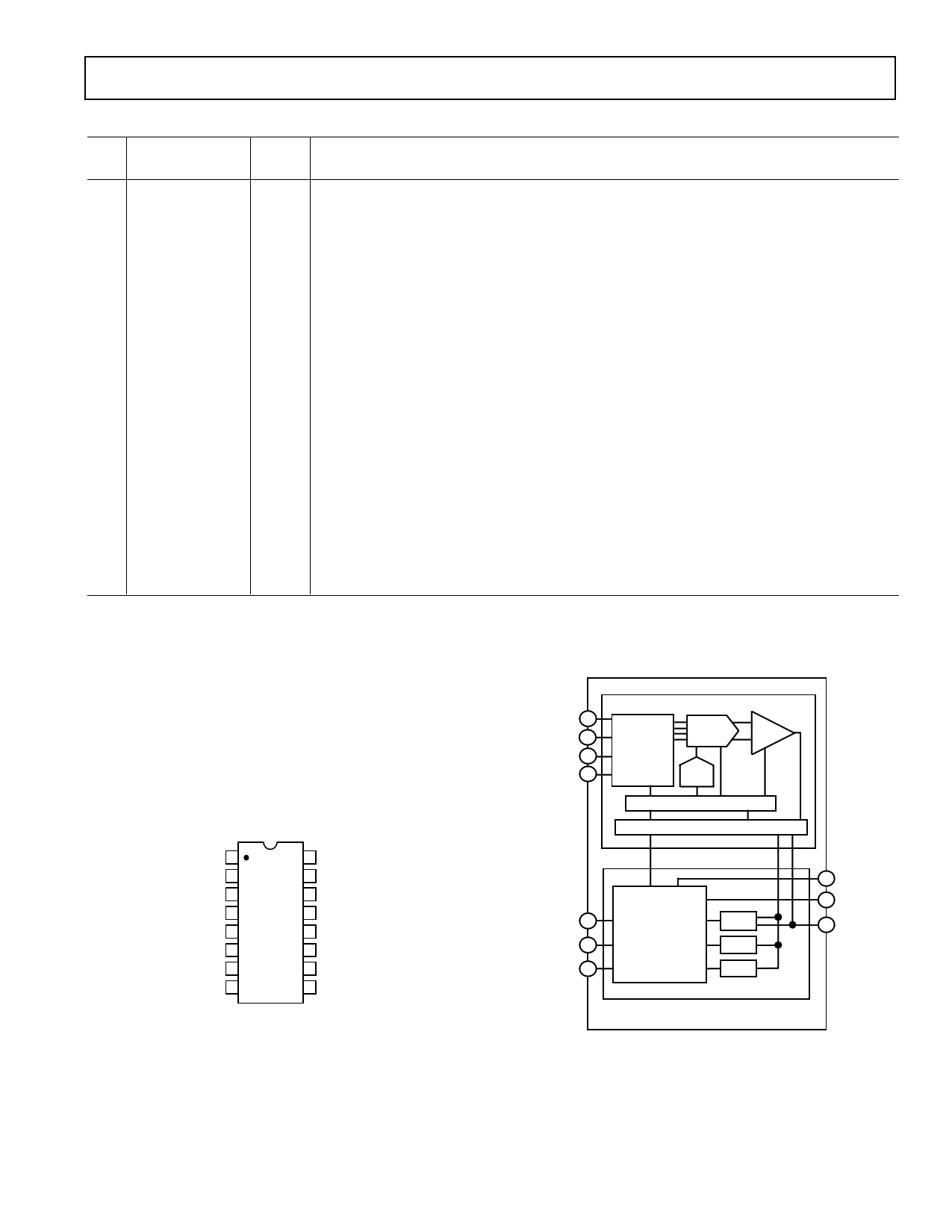
FUNCTIONAL BLOCK DIAGRAM
VIN 10
AGND SENSE 9
VREF 11
AGND 8
INPUT
BUFFERS
16-BIT
DAC
CAL
DAC
A CHIP
COMP
LOGIC TIMING
LEVEL TRANSLATORS
PRODUCT DESCRIPTION
The AD1876 is a 16-bit serial output sampling A/D converter
which uses a switched capacitor/charge redistribution architecture
to achieve a 100 kSPS conversion rate (10 µs total conversion
time). Overall performance is optimized by digitally correcting
internal nonlinearities through on-chip autocalibration.
The circuitry of the AD1876 is partitioned onto two monolithic
chips, a digital control chip fabricated with Analog Devices’
DSP CMOS process and an analog ADC chip fabricated with
the BiMOS II process. Both chips are contained in a single
package.
The serial output interface requires an external clock and
sample command signal. The output data rate may be as high
as 2.08 MHz, and is controlled by the external clock. The twos
complement format of the output data is MSB first and is di-
rectly compatible with the NPC SM5805 digital decimation fil-
ter used in consumer audio products. The AD1876 is also
compatible with a variety of DSP processors.
The AD1876 is packaged in a space saving 16-pin plastic DIP
and operates from +5 V and ± 12 V supplies; typical power con-
sumption is 235 mW. The digital supply (VDD) is isolated from
the linear supplies (VEE and VCC) for reduced digital crosstalk.
Separate analog and digital grounds are also provided.
CAL 16
CLK 2
SAMPLE 1
MICROCODED
CONTROLLER
SAR
ALU
15 BUSY
14 D OUT CLK
3 DOUT
RAM
D CHIP
AD1876
REV. A
Information furnished by Analog Devices is believed to be accurate and
reliable. However, no responsibility is assumed by Analog Devices for its
use, nor for any infringements of patents or other rights of third parties
which may result from its use. No license is granted by implication or
otherwise under any patent or patent rights of Analog Devices.
One Technology Way, P.O. Box 9106, Norwood, MA 02062-9106, U.S.A.
Tel: 617/329-4700
Fax: 617/326-8703
1 page 
AD1876
Pin
No. Name
1 SAMPLE
2 CLK
3 DOUT
4 DGND
5 VCC
6 N/C
7 N/C
8 AGND
9 AGND SENSE
10 VIN
11 VREF
12 VEE
13 VDD
14 DOUT CLK
15 BUSY
16 CAL
Type:
AI = Analog Input.
DI = Digital Input.
DO = Digital Output.
P = Power.
PIN DESCRIPTION
Type
DI
DI
DO
P
P
–
–
P/AI
AI
AI
AI
P
P
DO
DO
DI
Description
VIN Acquisition Control Pin. During conversion, SAMPLE controls the state of the internal
Sample-Hold Amplifier and initiates conversion (see “Conversion Control” paragraph). Dur-
ing calibration, SAMPLE is active HIGH, forcing DOUT (Pin 3) LOW. If SAMPLE is LOW
during calibration, DOUT will output diagnostic information (See “Autocalibration” paragraph.)
Master Clock Input. The AD1876 requires 17 clock pulses to execute a conversion. CLK is
also used to derive DOUT CLK (Pin 14). During calibration, 5000 clock pulses are applied.
Serial Output Data, Twos Complement format.
Digital Ground.
+12 V Analog Supply Voltage.
No Connection.
No Connection.
Analog Ground.
Analog Ground Sense.
Analog Input Voltage, referred the AGND SENSE.
External Voltage Reference Input, referred to AGND.
–12 V Analog Supply Voltage.
+5 V Logic Supply Voltage.
The rising edge of DOUT CLK may be used to latch DOUT (Pin 3). DOUT CLK is derived from
CLK.
Status Line for Converter. Active HIGH, indicating a conversion or calibration in progress.
Calibration Control Pin (asynchronous).
SAMPLE 1
16 CAL
CLK 2
15 BUSY
DOUT 3
14 DOUTCLK
DGND 4 AD1876 13 VDD
TOP VIEW
VCC 5 (Not to Scale) 12 VEE
NC 6
11 VREF
NC 7
10 VIN
AGND 8
9 AGND SENSE
NC = NO CONNECT
Package Pinout
VIN 10
AGND SENSE 9
VREF 11
AGND 8
INPUT
BUFFERS
16-BIT
DAC
CAL
DAC
A CHIP
COMP
LOGIC TIMING
LEVEL TRANSLATORS
CAL 16
CLK 2
SAMPLE 1
MICROCODED
CONTROLLER
SAR
ALU
15 BUSY
14 D OUT CLK
3 DOUT
RAM
D CHIP
AD1876
Functional Block Diagram
REV. A
–5–
5 Page 
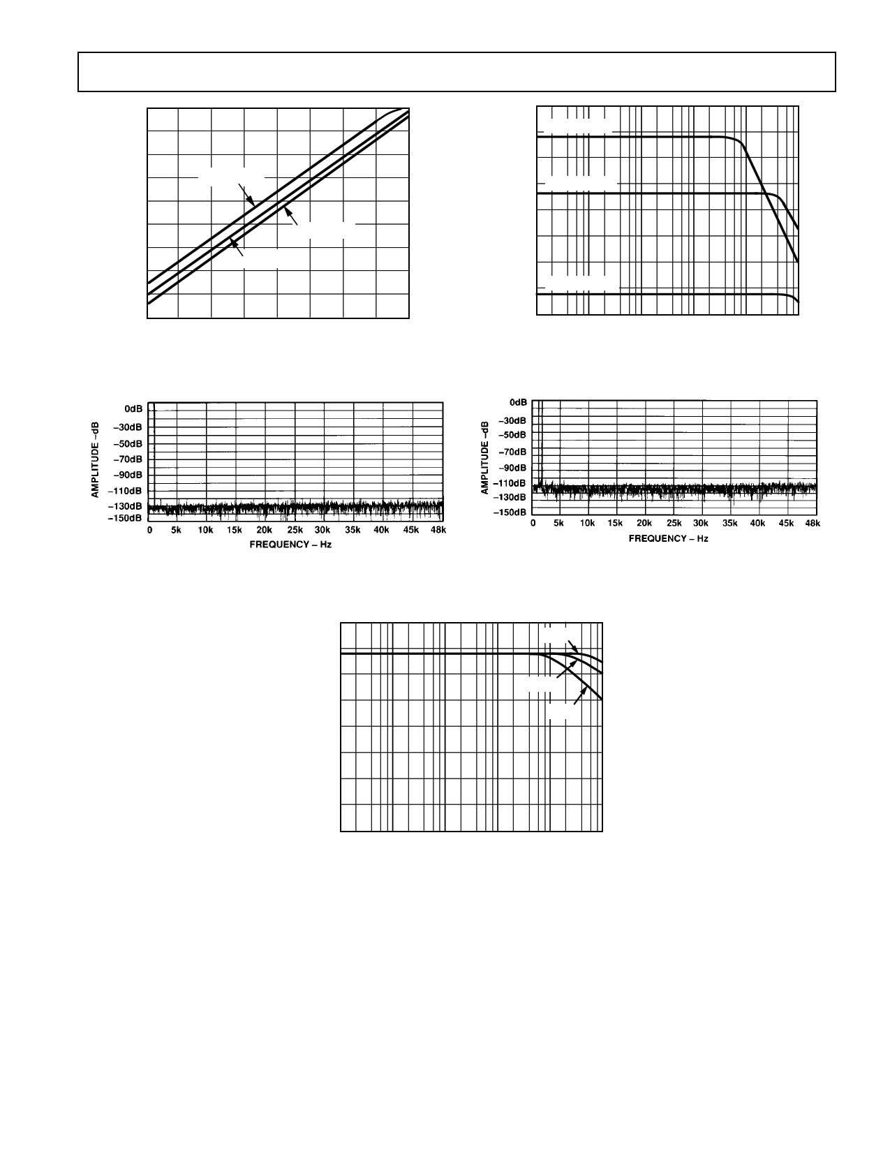
90
80
70
60 VREF = 10V
50
40 VREF = 5V
30
VREF = 7V
20
10
0
–80 –70 –60 –50 –40 –30 –20 –10
0
INPUT AMPLITUDE, REFERRED TO FULL-SCALE – dB
Figure 11. S/(N+D) vs. VREF vs. Input Amplitude
Typical Dynamic Performance–AD1876
90 –0dB INPUT
80
70 –20dB INPUT
60
50
40
30 –60dB INPUT
20
0
100 1k 10k 100k
INPUT FREQUENCY – Hz
1M
Figure 12. S/(N+D) vs. Input Frequency and Amplitude
Figure 13. 4096 Point FFT at 96 kSPS, fIN = 1.06 kHz
Figure 14. IMD Plot for fIN = 1008 Hz (fa), 1055 Hz (fb) at
96 kSPS
+5V
90
80
+12V
70
–12V
60
50
40
30
20
0
100
1k 10k
100k
RIPPLE FREQUENCY – Hz
1M
Figure 15. Power Supply Rejection (fIN = 1.06 kHz,
fSAMPLE = 96 kSPS, VRIPPLE = 0.3 V p-p)
REV. A
–11–
11 Page | ||
| Páginas | Total 12 Páginas | |
| PDF Descargar | [ Datasheet AD1876.PDF ] | |
Hoja de datos destacado
| Número de pieza | Descripción | Fabricantes |
| AD1870 | Single-Supply 16-Bit Stereo ADC | Analog Devices |
| AD1871 | Stereo Audio/ 24-Bit/ 96 kHz/ Multibit ADC | Analog Devices |
| AD1876 | 16-Bit 100 kSPS Sampling ADC | Analog Devices |
| AD1877 | Single-Supply 16-Bit Stereo ADC | Analog Devices |
| Número de pieza | Descripción | Fabricantes |
| SLA6805M | High Voltage 3 phase Motor Driver IC. |
Sanken |
| SDC1742 | 12- and 14-Bit Hybrid Synchro / Resolver-to-Digital Converters. |
Analog Devices |
|
DataSheet.es es una pagina web que funciona como un repositorio de manuales o hoja de datos de muchos de los productos más populares, |
| DataSheet.es | 2020 | Privacy Policy | Contacto | Buscar |
