|
|
|
PDF ACT-SF512K16N-39F18M Data sheet ( Hoja de datos )
| Número de pieza | ACT-SF512K16N-39F18M | |
| Descripción | ACT-SF512K16 High Speed 512Kx16 SRAM/FLASH Multichip Module | |
| Fabricantes | Aeroflex Circuit Technology | |
| Logotipo | ||
Hay una vista previa y un enlace de descarga de ACT-SF512K16N-39F18M (archivo pdf) en la parte inferior de esta página. Total 11 Páginas | ||
|
No Preview Available !
ACT–SF512K16 High Speed
512Kx16 SRAM/FLASH Multichip Module
FEATURES
CIRCUIT TECHNOLOGY
www.aeroflex.com
s 2 – 512K x 8 SRAMs & 2 – 512K x 8 Flash Die in
One MCM
s Access Times of 25ns (SRAM) and 60ns (Flash) or
35ns (SRAM) and 70 or 90ns (Flash)
s 512K x 16 SRAM
s 512K x 16 5V Flash
s Organized as 512K x 16 of SRAM and 512K x 16 of
Flash Memory with Separate Data Buses
s Both Blocks of Memory are User Configurable as
1M x 8
s Low Power CMOS
s Input and Output TTL Compatible Design
s MIL-PRF-38534 Compliant MCMs Available
s Decoupling Capacitors and Multiple Grounds for Low
Noise
s Industrial and Military Temperature Ranges
s Industry Standard Pinouts
Note: Programming information available upon request
s Packaging – Hermetic Ceramic
q 66 Pin, 1.08" x 1.08" x .160" PGA Type, No Shoulder,
Aeroflex code# "P3"
q 66 Pin, 1.08" x 1.08" x .185" PGA Type, With
Shoulder, Aeroflex code# "P7"
q 68 Lead, .94" x .94" x .140" Single-Cavity Small
Outline Gull Wing, Aeroflex code# "F18" (Drops into
the 68 Lead JEDEC .99"SQ CQFJ footprint)
s DESC SMD Pending – 5962-96901
FLASH MEMORY FEATURES
s Sector Architecture (Each Die)
q 8 Equal Sectors of 64K bytes each
q Any combination of sectors can be erased with one
command sequence.
s +5V Programing, 5V ±10% Supply
s Embedded Erase and Program Algorithms
s Hardware and Software Write Protection
s Internal Program Control Time.
s 10,000 Erase / Program Cycles
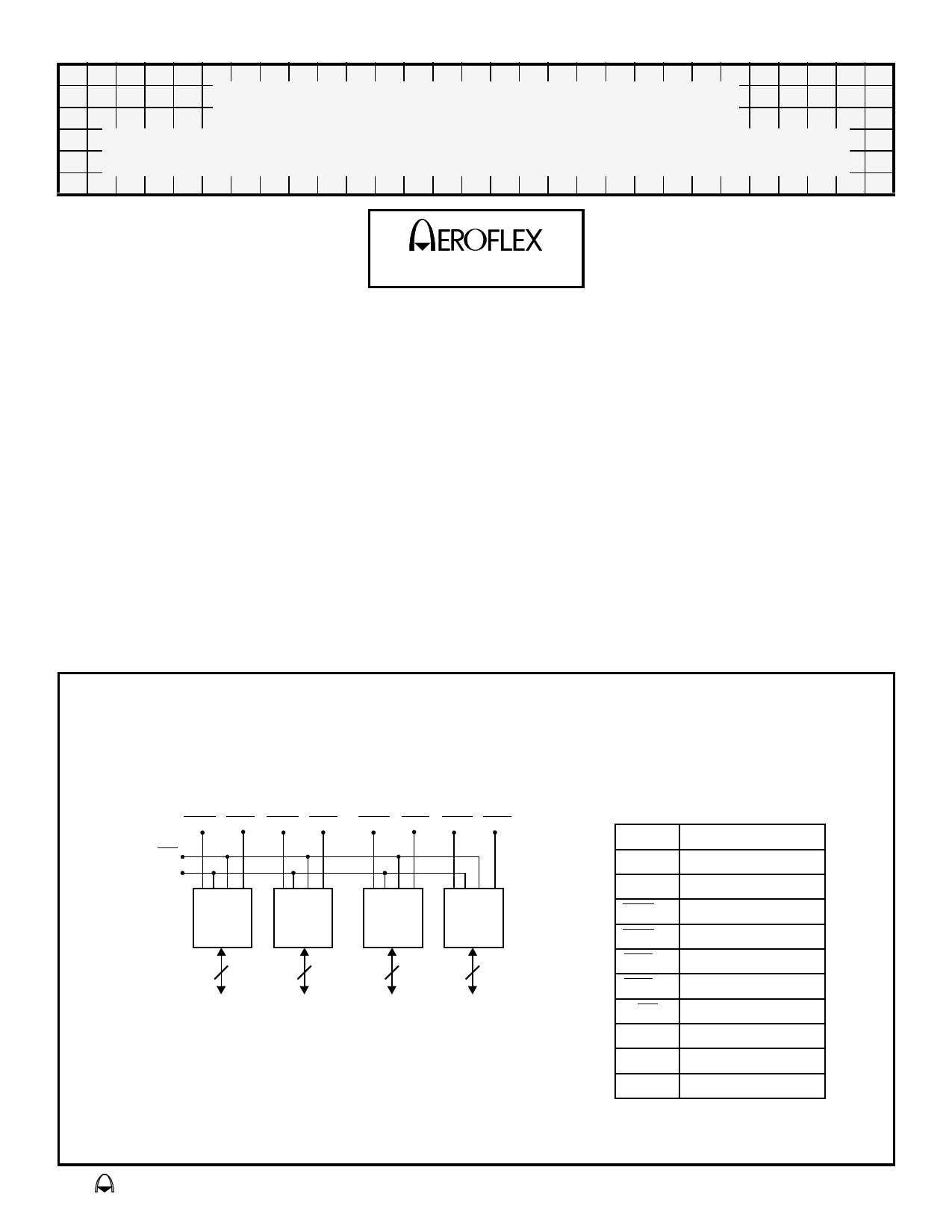
Block Diagram – PGA Type Packages (P3 & P7) & CQFP (F18)
SWE1 SCE1 SWE2 SCE2 FWE1 FCE1 FWE2 FCE2
OE
A0 – A18
512Kx8
SRAM
512Kx8
SRAM
512Kx8
Flash
512Kx8
Flash
8
SI/O0-7
8
SI/O8-15
8
FI/O0-7
8
FI/O8-15
Pin Description
FI/O0-15 Flash Data I/O
SI/O0-15 SRAM Data I/O
A0–18
Address Inputs
FWE1-2 Flash Write Enables
SWE1-2 SRAM Write Enables
FCE1-2 Flash Chip Enables
SCE1-2 SRAM Chip Enables
OE Output Enable
NC Not Connected
VCC Power Supply
GND
Ground
eroflex Circuit Technology - Advanced Multichip Modules © SCD1663 REV A 4/28/98
1 page 
Flash AC Characteristics – Read Only Operations
(Vcc = 5.0V, Vss = 0V, Tc = -55°C to +125°C)
Parameter
Symbol
–60 –70 –90
Units
JEDEC Stand’d Min Max Min Max Min Max
Read Cycle Time
Address Access Time
Chip Enable Access Time
Output Enable to Output Valid
Chip Enable to Output High Z (1)
Output Enable High to Output High Z(1)
Output Hold from Address, CE or OE Change, Whichever is First
tAVAV
tAVQV
tELQV
tGLQV
tEHQZ
tGHQZ
tAXQX
tRC 60 70 90
ns
tACC 60 70 90 ns
tCE 60 70 90 ns
tOE 30 35 35 ns
tDF 20 20 20 ns
tDF 20 20 20 ns
tOH 0 0 0
ns
Note 1. Guaranteed by design, but not tested
Flash AC Characteristics – Write / Erase / Program Operations, FWE Controlled
(Vcc = 5.0V, Vss = 0V, Tc = -55°C to +125°C)
Parameter
Symbol
–60 –70 –90
Units
JEDEC Stand’d Min Max Min Max Min Max
Write Cycle Time
Chip Enable Setup Time
Write Enable Pulse Width
Address Setup Time
Data Setup Time
Data Hold Time
Address Hold Time
Write Enable Pulse Width High
Duration of Byte Programming Operation
Sector Erase Time
Read Recovery Time before Write
Vcc Setup Time
Chip Programming Time
Chip Enable Hold Time
Chip Erase Time
tAVAC
tELWL
tWLWH
tAVWL
tDVWH
tWHDX
tWLAX
tWHWL
tWHWH1
tWHWH2
tGHWL
tWHWH3
tWC
tCE
tWP
tAS
tDS
tDH
tAH
tWPH
tVCE
tOEH 1
60 70 90
000
40 45 45
000
40 45 45
000
45 45 45
20 20 20
14 TYP 14 TYP 14 TYP
30 30 30
000
50 50 50
50 50 50
10 10 10
120 120 120
ns
ns
ns
ns
ns
ns
ns
ns
µs
Sec
µs
µs
Sec
ns
Sec
1. Toggle and Data Polling only.
Flash AC Characteristics – Write / Erase / Program Operations, FCE Controlled
(Vcc = 5.0V, Vss = 0V, Tc = -55°C to +125°C)
Parameter
Symbol
–60 –70 –90
Units
JEDEC Stand’d Min Max Min Max Min Max
Write Cycle Time
tAVAC
tWC 60
70
90
ns
Write Enable Setup Time
tWLEL
tWS 0
0
0
ns
Chip Enable Pulse Width
tELEH
tCP 40
45
45
ns
Address Setup Time
tAVEL
tAS 0
0
0
ns
Data Setup Time
tDVEH
tDS 40
45
45
ns
Data Hold Time
tEHDX
tDH 0
0
0
ns
Address Hold Time
tELAX
tAH 45
45
45
ns
Chip Enable Pulse Width High
tEHEL
tCPH
20
20
20
ns
Duration of Byte Programming
tWHWH1
14 TYP 14 TYP 14 TYP µs
Sector Erase Time
Read Recovery Time
tWHWH2
tGHEL
30 30 30
000
Sec
ns
Chip Programming Time
50 50 50 Sec
Chip Erase Time
tWHWH3
120 120 120 Sec
Aeroflex Circuit Technology
5 SCD1663 REV A 4/28/98 Plainview NY (516) 694-6700
5 Page 
CIRCUIT TECHNOLOGY
Ordering Information
Model Number
DESC SMD Number
Speed
ACT–SF512K16N–26P3Q
5462-96901 (Pending)
25(S) / 60(F) ns
ACT–SF512K16N–37P3Q
5462-96901 (Pending)
35(S) / 70(F) ns
ACT–SF512K16N–39P3Q
5462-96901 (Pending)
35(S) / 90(F) ns
ACT–SF512K16N–26P7Q
5462-96901 (Pending)
25(S) / 60(F) ns
ACT–SF512K16N–37P7Q
5462-96901 (Pending)
35(S) / 70(F) ns
ACT–SF512K16N–39P7Q
5462-96901 (Pending)
35(S) / 90(F) ns
ACT–SF512K16N–26F18Q
5462-96901 (Pending)
25(S) / 60(F) ns
ACT–SF512K16N–37F18Q
5462-96901 (Pending)
35(S) / 70(F) ns
ACT–SF512K16N–39F18Q
5462-96901 (Pending)
Note: (S) = Speed for SRAM, (F) = Speed for FLASH
35(S) / 90(F) ns
Package
1.08"sq PGA-Type
1.08"sq PGA-Type
1.08"sq PGA-Type
1.08"sq PGA-Type
1.08"sq PGA-Type
1.08"sq PGA-Type
.94"sq CQFP
.94"sq CQFP
.94"sq CQFP
Part Number Breakdown
ACT– S F 512K 16 N– 26 P7 Q
Aeroflex Circuit
Technology
Screening
Memory Type
S (SRAM) & F (FLASH) Combo
Memory Depth
C = Commercial Temp, 0°C to +70°C
I = Industrial Temp, -40°C to +85°C
T = Military Temp, -55°C to +125°C
M = Military Temp, -55°C to +125°C, Screening *
Q = MIL-PRF-38534 Compliant / SMD
Options, N = none
Memory Width, Bits
Memory Speed Code
26 = 25ns SRAM & 60ns FLASH
37 = 35ns SRAM & 70ns FLASH
39 = 35ns SRAM & 90ns FLASH
Package Type & Size
Surface Mount Packages
Thru-Hole Packages
F18 = .94"SQ 68 Lead Dual-Cavity P3 = 1.085"SQ PGA 66 Pins
CQFP
with out shoulder
P7 = 1.085"SQ PGA 66 Pins
with shoulder
* Screened to the individual test methods of MIL-STD-883
Specifications subject to change without notice.
Aeroflex Circuit Technology
35 South Service Road
Plainview New York 11830
Aeroflex Circuit Technology
Telephone: (516) 694-6700
FAX:
(516) 694-6715
Toll Free Inquiries: 1-(800) 843-1553
11 SCD1663 REV A 4/28/98 Plainview NY (516) 694-6700
11 Page | ||
| Páginas | Total 11 Páginas | |
| PDF Descargar | [ Datasheet ACT-SF512K16N-39F18M.PDF ] | |
Hoja de datos destacado
| Número de pieza | Descripción | Fabricantes |
| ACT-SF512K16N-39F18C | ACT-SF512K16 High Speed 512Kx16 SRAM/FLASH Multichip Module | Aeroflex Circuit Technology |
| ACT-SF512K16N-39F18I | ACT-SF512K16 High Speed 512Kx16 SRAM/FLASH Multichip Module | Aeroflex Circuit Technology |
| ACT-SF512K16N-39F18M | ACT-SF512K16 High Speed 512Kx16 SRAM/FLASH Multichip Module | Aeroflex Circuit Technology |
| ACT-SF512K16N-39F18Q | ACT-SF512K16 High Speed 512Kx16 SRAM/FLASH Multichip Module | Aeroflex Circuit Technology |
| Número de pieza | Descripción | Fabricantes |
| SLA6805M | High Voltage 3 phase Motor Driver IC. |
Sanken |
| SDC1742 | 12- and 14-Bit Hybrid Synchro / Resolver-to-Digital Converters. |
Analog Devices |
|
DataSheet.es es una pagina web que funciona como un repositorio de manuales o hoja de datos de muchos de los productos más populares, |
| DataSheet.es | 2020 | Privacy Policy | Contacto | Buscar |