|
|
|
PDF AD5321 Data sheet ( Hoja de datos )
| Número de pieza | AD5321 | |
| Descripción | +2.5 V to +5.5 V/ 120 uA/ 2-Wire Interface/ Voltage Output 8-/10-/12-Bit DACs | |
| Fabricantes | Analog Devices | |
| Logotipo | ||
Hay una vista previa y un enlace de descarga de AD5321 (archivo pdf) en la parte inferior de esta página. Total 15 Páginas | ||
|
No Preview Available !
a +2.5 V to +5.5 V, 120 A, 2-Wire Interface,
Voltage Output 8-/10-/12-Bit DACs
AD5301/AD5311/AD5321*
FEATURES
AD5301: Buffered Voltage Output 8-Bit DAC
AD5311: Buffered Voltage Output 10-Bit DAC
AD5321: Buffered Voltage Output 12-Bit DAC
6-Lead SOT-23 and 8-Lead SOIC Packages
Micropower Operation: 120 A @ 3 V
2-Wire (I2C® Compatible) Serial Interface
Data Readback Capability
+2.5 V to +5.5 V Power Supply
Guaranteed Monotonic By Design Over All Codes
Power-Down to 50 nA @ 3 V
Reference Derived from Power Supply
Power-On-Reset to Zero Volts
On-Chip Rail-to-Rail Output Buffer Amplifier
Three Power-Down Functions
APPLICATIONS
Portable Battery Powered Instruments
Digital Gain and Offset Adjustment
Programmable Voltage and Current Sources
Programmable Attenuators
GENERAL DESCRIPTION
The AD5301/AD5311/AD5321 are single 8-, 10- and 12-bit
buffered voltage-output DACs that operate from a single +2.5 V
to +5.5 V supply consuming 120 µA at 3 V. The on-chip output
amplifier allows rail-to-rail output swing with a slew rate of
0.7 V/µs. It uses a 2-wire (I2C compatible) serial interface that
operates at clock rates up to 400 kHz. Multiple devices can
share the same bus.
The reference for the DAC is derived from the power supply
inputs and thus gives the widest dynamic output range. These
parts incorporate a power-on-reset circuit, which ensures that
the DAC output powers-up to zero volts and remains there until
a valid write takes place. The parts contain a power-down feature
which reduces the current consumption of the device to 50 nA
at 3 V and provides software-selectable output loads while in
power-down mode.
The low power consumption in normal operation make these
DACs ideally suited to portable battery-operated equipment.
The power consumption is 0.75 mW at 5 V, 0.36 mW at 3 V
reducing to 1 µW in all power-down modes.
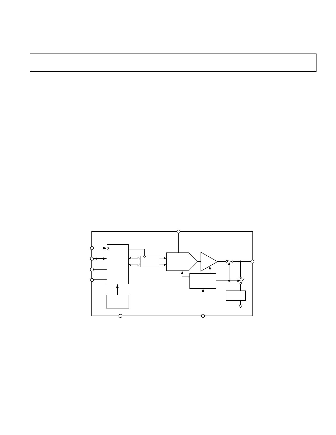
FUNCTIONAL BLOCK DIAGRAM
VDD
AD5301/AD5311/AD5321
SCL
REF
SDA
A0
A1*
INTERFACE
LOGIC
DAC
REGISTER
8-/10-/12-BIT
DAC
BUFFER
POWER-DOWN
LOGIC
VOUT
POWER-ON
RESET
RESISTOR
NETWORK
GND
*AVAILABLE ON 8-LEAD VERSION ONLY
PD*
I2C is a registered trademark of Philips Corporation.
*Protected by U.S. Patent No. 5684481, other patent pending.
REV. 0
Information furnished by Analog Devices is believed to be accurate and
reliable. However, no responsibility is assumed by Analog Devices for its
use, nor for any infringements of patents or other rights of third parties
which may result from its use. No license is granted by implication or
otherwise under any patent or patent rights of Analog Devices.
One Technology Way, P.O. Box 9106, Norwood, MA 02062-9106, U.S.A.
Tel: 781/329-4700 World Wide Web Site: http://www.analog.com
Fax: 781/326-8703
© Analog Devices, Inc., 1999
1 page 
AD5301/AD5311/AD5321
SOIC
Pin No.
1
2
3
4
5
6
7
8
PIN FUNCTION DESCRIPTION
SOT-23
Pin No.
6
5
N/A
4
N/A
3
2
1
Mnemonic
VDD
A0
A1
VOUT
PD
SCL
SDA
GND
Function
Power Supply Input. These parts can be operated from +2.5 V to +5.5 V and the supply
should be decoupled with a 10 µF in parallel with a 0.1 µF capacitor to GND.
Address Input. Sets the Least Significant Bit of the 7-bit slave address.
Address Input. Sets the 2nd Least Significant Bit of the 7-bit slave address.
Buffered analog output voltage from the DAC. The output amplifier has rail-to-rail operation.
Active low control input that acts as a hardware power-down option. This pin overrides any
software power-down option. The DAC output goes three-state and the current consumption
of the part drops to 50 nA @ 3 V (200 nA @ 5 V).
Serial Clock Line. This is used in conjunction with the SDA line to clock data into the 16-bit
input shift register. Clock rates of up to 400 kbit/s can be accommodated in the I2C compat-
ible interface. SCL may be CMOS/TTL driven.
Serial Data Line. This is used in conjunction with the SCL line to clock data into the 16-bit
input shift register during the write cycle and used to read back one or two bytes of data
(one byte for the AD5301, two bytes for the AD5311/AD5321) during the read cycle. It is
a bidirectional open-drain data line that should be pulled to the supply with an external
pull-up resistor. If not used in readback mode, SDA may be CMOS/TTL driven.
Ground reference point for all circuitry on the part.
PIN CONFIGURATIONS
6-Lead SOT-23
(RT-6)
8-Lead SOIC
(RM-8)
AD5301/AD5311/AD5321
GND 1
6 VDD
SDA 2 TOP VIEW 5 A0
(Not to Scale)
SCL 3
4 VOUT
AD5301/AD5311/AD5321
VDD 1
8 GND
A0 2 TOP VIEW 7 SDA
A1 3 (Not to Scale) 6 SCL
VOUT 4
5 PD
REV. 0
–5–
5 Page 
AD5301/AD5311/AD5321
WRITE OPERATION
When writing to the AD5301/AD5311/AD5321 DACs, the user
must begin with an address byte, after which the DAC will
acknowledge that it is prepared to receive data by pulling SDA
low. This address byte is followed by the 16-bit word in the
form of two control bytes. The write operations for the three
DACs are shown in the figures below.
SCL
SDA
0
START
COND
BY
MASTER
SCL
00
11
ADDRESS BYTE
A1* A0 R/W
X
ACK
BY
AD5301
X PD1 PD0 D7 D6 D5
MOST SIGNIFICANT CONTROL BYTE
D4
ACK
BY
AD5301
SDA
D3 D2 D1 D0
X
X
X
LEAST SIGNIFICANT CONTROL BYTE
*THIS BIT MUST BE 0 IN THE 6-PIN SOT-23 VERSION.
X
ACK STOP
BY COND
AD5301 BY
MASTER
Figure 24. AD5301 Write Sequence
SCL
SDA
0
START
COND
BY
MASTER
SCL
00
1
ADDRESS
BYTE
1 A1* A0 R/W
X
ACK
BY
AD5311
X PD1 PD0 D9 D8 D7
MOST SIGNIFICANT CONTROL BYTE
D6
ACK
BY
AD5311
SDA
D5 D4 D3 D2 D1 D0
X
X
LEAST SIGNIFICANT CONTROL BYTE
*THIS BIT MUST BE 0 IN THE 6-PIN SOT-23 VERSION.
ACK STOP
BY COND
AD5311 BY
MASTER
Figure 25. AD5311 Write Sequence
SCL
SDA
0
START
COND
BY
MASTER
SCL
00
11
ADDRESS BYTE
A1* A0 R/W
X
ACK
BY
AD5321
X PD1 PD0 D11 D10 D9
MOST SIGNIFICANT CONTROL BYTE
D8
ACK
BY
AD5321
SDA
D7 D6 D5 D4 D3 D2 D1 D0
LEAST SIGNIFICANT CONTROL BYTE
*THIS BIT MUST BE 0 IN THE 6-PIN SOT-23 VERSION.
ACK STOP
BY COND
AD5321 BY
MASTER
Figure 26. AD5321 Write Sequence
REV. 0
–11–
11 Page | ||
| Páginas | Total 15 Páginas | |
| PDF Descargar | [ Datasheet AD5321.PDF ] | |
Hoja de datos destacado
| Número de pieza | Descripción | Fabricantes |
| AD532 | Internally Trimmed Integrated Circuit Multiplier | Analog Devices |
| AD5320 | +2.7 V to +5.5 V/ 140 uA/ Rail-to-Rail Output 12-Bit DAC in a SOT-23 | Analog Devices |
| AD5321 | +2.5 V to +5.5 V/ 120 uA/ 2-Wire Interface/ Voltage Output 8-/10-/12-Bit DACs | Analog Devices |
| AD5322 | +2.5 V to +5.5 V/ 230 uA Dual Rail-to-Rail/ Voltage Output 8-/10-/12-Bit DACs | Analog Devices |
| Número de pieza | Descripción | Fabricantes |
| SLA6805M | High Voltage 3 phase Motor Driver IC. |
Sanken |
| SDC1742 | 12- and 14-Bit Hybrid Synchro / Resolver-to-Digital Converters. |
Analog Devices |
|
DataSheet.es es una pagina web que funciona como un repositorio de manuales o hoja de datos de muchos de los productos más populares, |
| DataSheet.es | 2020 | Privacy Policy | Contacto | Buscar |