|
|
|
PDF AD5312 Data sheet ( Hoja de datos )
| Número de pieza | AD5312 | |
| Descripción | +2.5 V to +5.5 V/ 230 uA Dual Rail-to-Rail/ Voltage Output 8-/10-/12-Bit DACs | |
| Fabricantes | Analog Devices | |
| Logotipo | ||
Hay una vista previa y un enlace de descarga de AD5312 (archivo pdf) en la parte inferior de esta página. Total 16 Páginas | ||
|
No Preview Available !
a +2.5 V to +5.5 V, 230 A Dual Rail-to-Rail,
Voltage Output 8-/10-/12-Bit DACs
AD5302/AD5312/AD5322*
FEATURES
AD5302: Two 8-Bit Buffered DACs in One Package
AD5312: Two 10-Bit Buffered DACs in One Package
AD5322: Two 12-Bit Buffered DACs in One Package
10-Lead SOIC Package
Micropower Operation: 300 A @ 5 V (Including
Reference Current)
Power-Down to 200 nA @ 5 V, 50 nA @ 3 V
+2.5 V to +5.5 V Power Supply
Double-Buffered Input Logic
Guaranteed Monotonic By Design Over All Codes
Buffered/Unbuffered Reference Input Options
0–VREF Output Voltage
Power-On-Reset to Zero Volts
Simultaneous Update of DAC Outputs via LDAC
Low Power Serial Interface with Schmitt-Triggered
Inputs
On-Chip Rail-to-Rail Output Buffer Amplifiers
APPLICATIONS
Portable Battery-Powered Instruments
Digital Gain and Offset Adjustment
Programmable Voltage and Current Sources
Programmable Attenuators
GENERAL DESCRIPTION
The AD5302/AD5312/AD5322 are dual 8-, 10- and 12-bit buff-
ered voltage output DACs in a 10-lead µSOIC package that
operate from a single +2.5 V to +5.5 V supply consuming
230 µA at 3 V. Their on-chip output amplifiers allow the outputs
to swing rail-to-rail with a slew rate of 0.7 V/µs. The AD5302/
AD5312/AD5322 utilize a versatile 3-wire serial interface which
operates at clock rates up to 30 MHz and is compatible with
standard SPI™, QSPI™, MICROWIRE™ and DSP interface
standards.
The references for the two DACs are derived from two reference
pins (one per DAC). The reference inputs may be configured as
buffered or unbuffered inputs. The outputs of both DACs may
be updated simultaneously using the asynchronous LDAC in-
put. The parts incorporate a power-on-reset circuit that ensures
that the DAC outputs power-up to 0 V and remain there until a
valid write takes place to the device. The parts contain a power-
down feature that reduces the current consumption of the
devices to 200 nA at 5 V (50 nA at 3 V) and provides software-
selectable output loads while in power-down mode.
The low power consumption of these parts in normal operation
make them ideally suited to portable battery operated equip-
ment. The power consumption is 1.5 mW at 5 V, 0.7 mW at
3 V, reducing to 1 µW in power-down mode.
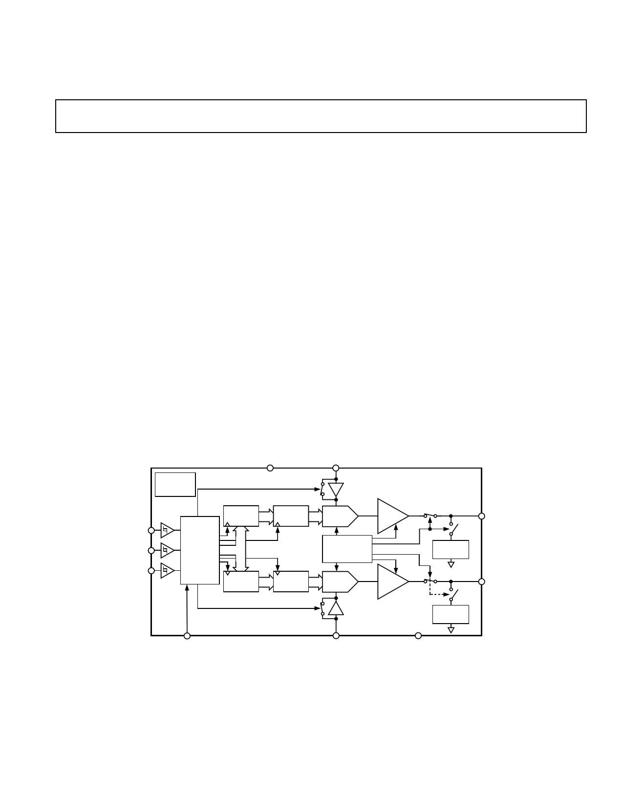
POWER-ON
RESET
FUNCTIONAL BLOCK DIAGRAM
VDD
VREFA
AD5302/AD5312/AD5322
SYNC
SCLK
DIN
INPUT
REGISTER
INTERFACE
LOGIC
DAC
REGISTER
STRING
DAC
BUFFER
POWER-DOWN
LOGIC
INPUT
REGISTER
DAC
REGISTER
STRING
DAC
BUFFER
VOUTA
RESISTOR
NETWORK
VOUTB
RESISTOR
NETWORK
LDAC
VREFB
GND
*Patent Pending; protected by U.S. Patent No. 5684481.
SPI and QSPI are trademarks of Motorola, Inc.
MICROWIRE is a trademark of National Semiconductor Corporation.
REV. 0
Information furnished by Analog Devices is believed to be accurate and
reliable. However, no responsibility is assumed by Analog Devices for its
use, nor for any infringements of patents or other rights of third parties
which may result from its use. No license is granted by implication or
otherwise under any patent or patent rights of Analog Devices.
One Technology Way, P.O. Box 9106, Norwood, MA 02062-9106, U.S.A.
Tel: 781/329-4700 World Wide Web Site: http://www.analog.com
Fax: 781/326-8703
© Analog Devices, Inc., 1999
1 page 
AD5302/AD5312/AD5322
Pin No. Mnemonic
1 LDAC
2 VDD
3 VREFB
4 VREFA
5 VOUTA
6 VOUTB
7 SYNC
8 SCLK
9 DIN
10 GND
PIN FUNCTION DESCRIPTIONS
Function
Active low control input that transfers the contents of the input registers to their respective DAC regis-
ters. Pulsing this pin low allows either or both DAC registers to be updated if the input registers have new
data. This allows simultaneous update of both DAC outputs
Power Supply Input. These parts can be operated from +2.5 V to +5.5 V and the supply should be de-
coupled to GND.
Reference Input Pin for DAC B. This is the reference for DAC B. It may be configured as a buffered or
an unbuffered input, depending on the BUF bit in the control word of DAC B. It has an input range
from 0 V to VDD in unbuffered mode and from 1 V to VDD in buffered mode.
Reference Input Pin for DAC A. This is the reference for DAC A. It may be configured as a buffered or
an unbuffered input depending on the BUF bit in the control word of DAC A. It has an input range from
0 V to VDD in unbuffered mode and from 1 V to VDD in buffered mode.
Buffered Analog Output Voltage from DAC A. The output amplifier has rail-to-rail operation.
Buffered Analog Output Voltage from DAC B. The output amplifier has rail-to-rail operation.
Active Low Control Input. This is the frame synchronization signal for the input data. When SYNC goes
low, it powers on the SCLK and DIN buffers and enables the input shift register. Data is transferred in
on the falling edges of the following 16 clocks. If SYNC is taken high before the 16th falling edge, the
rising edge of SYNC acts as an interrupt and the write sequence is ignored by the device.
Serial Clock Input. Data is clocked into the input shift register on the falling edge of the serial clock in-
put. Data can be transferred at rates up to 30 MHz. The SCLK input buffer is powered down after each
write cycle.
Serial Data Input. This device has a 16-bit input shift register. Data is clocked into the register on the
falling edge of the serial clock input. The DIN input buffer is powered down after each write cycle.
Ground reference point for all circuitry on the part.
TERMINOLOGY
RELATIVE ACCURACY
For the DAC, relative accuracy or Integral Nonlinearity (INL)
is a measure of the maximum deviation, in LSBs, from a straight
line passing through the actual endpoints of the DAC transfer
function. A typical INL vs. code plot can be seen in Figure 4.
DIFFERENTIAL NONLINEARITY
Differential Nonlinearity (DNL) is the difference between the
measured change and the ideal 1 LSB change between any two
adjacent codes. A specified differential nonlinearity of ± 1 LSB
maximum ensures monotonicity. This DAC is guaranteed
monotonic by design. A typical DNL vs. code plot can be seen
in Figure 7.
OFFSET ERROR
This is a measure of the offset error of the DAC and the output
amplifier. It is expressed as a percentage of the full-scale range.
GAIN ERROR
This is a measure of the span error of the DAC. It is the devia-
tion in slope of the actual DAC transfer characteristic from the
ideal expressed as a percentage of the full-scale range.
OFFSET ERROR DRIFT
This is a measure of the change in offset error with changes in
temperature. It is expressed in (ppm of full-scale range)/°C.
GAIN ERROR DRIFT
This is a measure of the change in gain error with changes in tem-
perature. It is expressed in (ppm of full-scale range)/°C.
MAJOR-CODE TRANSITION GLITCH ENERGY
Major-code transition glitch energy is the energy of the impulse
injected into the analog output when the code in the DAC regis-
ter changes state. It is normally specified as the area of the glitch
in nV-secs and is measured when the digital code is changed by
1 LSB at the major carry transition (011 . . . 11 to 100 . . . 00 or
100 . . . 00 to 011 . . . 11).
DIGITAL FEEDTHROUGH
Digital feedthrough is a measure of the impulse injected into the
analog output of the DAC from the digital input pins of the
device, but is measured when the DAC is not being written to
(SYNC held high). It is specified in nV-secs and is measured
with a full-scale change on the digital input pins, i.e., from all 0s
to all 1s and vice versa.
ANALOG CROSSTALK
This is the glitch impulse transferred to the output of one DAC
due to a change in the output of the other DAC. It is measured
by loading one of the input registers with a full-scale code change
(all 0s to all 1s and vice versa) while keeping LDAC high. Then
pulse LDAC low and monitor the output of the DAC whose
digital code was not changed. The area of the glitch is expressed
in nV-secs.
REV. 0
–5–
5 Page 
SERIAL INTERFACE
The AD5302/AD5312/AD5322 are controlled over a versatile,
3-wire serial interface, which operates at clock rates up to 30 MHz
and is compatible with SPI, QSPI, MICROWIRE and DSP
interface standards.
Input Shift Register
The input shift register is 16 bits wide (see Figures 28–30 below).
Data is loaded into the device as a 16-bit word under the con-
trol of a serial clock input, SCLK. The timing diagram for this
operation is shown in Figure 1. The 16-bit word consists of four
control bits followed by 8, 10 or 12 bits of DAC data, depend-
ing on the device type. The first bit loaded is the MSB (Bit 15),
which determines whether the data is for DAC A or DAC B. Bit
14 determines if the reference input will be buffered or unbuf-
fered. Bits 13 and 12 control the operating mode of the DAC.
Bit Name
15 A/B
14 BUF
13 PD1
12 PD0
Table I. Control Bits
Function
0: Data Written to DAC A
1: Data Written to DAC B
0: Reference Is Unbuffered
1: Reference Is Buffered
Mode Bit
Mode Bit
Power-On
Default
N/A
0
0
0
DB15 (MSB)
A/B BUF PD1 PD0 D7 D6 D5 D4 D3 D2 D1 D0
X
DB0 (LSB)
XXX
DATA BITS
Figure 28. AD5302 Input Shift Register Contents
DB15 (MSB)
DB0 (LSB)
A/B BUF PD1 PD0 D9 D8 D7 D6 D5 D4 D3 D2 D1 D0 X X
DATA BITS
Figure 29. AD5312 Input Shift Register Contents
DB15 (MSB)
DB0 (LSB)
A/B BUF PD1 PD0 D11 D10 D9 D8 D7 D6 D5 D4 D3 D2 D1 D0
DATA BITS
Figure 30. AD5322 Input Shift Register Contents
The remaining bits are DAC data bits, starting with the MSB
and ending with the LSB. The AD5322 uses all 12 bits of DAC
data, the AD5312 uses 10 bits and ignores the 2 LSBs. The
AD5302 uses eight bits and ignores the last four bits. The data
format is straight binary, with all zeroes corresponding to
0 V output, and all ones corresponding to full-scale output
(VREF – 1 LSB).
AD5302/AD5312/AD5322
The SYNC input is a level-triggered input that acts as a frame
synchronization signal and chip enable. Data can only be trans-
ferred into the device while SYNC is low. To start the serial
data transfer, SYNC should be taken low observing the mini-
mum SYNC to SCLK active edge setup time, t4. After SYNC
goes low, serial data will be shifted into the device’s input shift
register on the falling edges of SCLK for 16 clock pulses. Any
data and clock pulses after the 16th will be ignored, and no
further serial data transfer will occur until SYNC is taken high
and low again.
SYNC may be taken high after the falling edge of the 16th
SCLK pulse, observing the minimum SCLK falling edge to
SYNC rising edge time, t7.
After the end of serial data transfer, data will automatically be
transferred from the input shift register to the input register of
the selected DAC. If SYNC is taken high before the 16th falling
edge of SCLK, the data transfer will be aborted and the input
registers will not be updated.
When data has been transferred into both input registers, the
DAC registers of both DACs may be simultaneously updated,
by taking LDAC low.
Low Power Serial Interface
To reduce the power consumption of the device even further,
the interface only powers up fully when the device is being writ-
ten to. As soon as the 16-bit control word has been written to
the part, the SCLK and DIN input buffers are powered down.
They only power-up again following a falling edge of SYNC.
Double-Buffered Interface
The AD5302/AD5312/AD5322 DACs all have double-buffered
interfaces consisting of two banks of registers—input registers
and DAC registers. The input register is connected directly to
the input shift register and the digital code is transferred to the
relevant input register on completion of a valid write sequence.
The DAC register contains the digital code used by the resistor
string.
Access to the DAC register is controlled by the LDAC function.
When LDAC is high, the DAC register is latched and the input
register may change state without affecting the contents of the
DAC register. However, when LDAC is brought low, the DAC
register becomes transparent and the contents of the input regis-
ter are transferred to it.
This is useful if the user requires simultaneous updating of both
DAC outputs. The user may write to both input registers indi-
vidually and then, by pulsing the LDAC input low, both outputs
will update simultaneously.
These parts contain an extra feature whereby the DAC register
is not updated unless its input register has been updated since
the last time that LDAC was brought low. Normally, when
LDAC is brought low, the DAC registers are filled with the
contents of the input registers. In the case of the AD5302/AD5312/
AD5322, the part will only update the DAC register if the input
register has been changed since the last time the DAC register
was updated thereby removing unnecessary digital crosstalk.
REV. 0
–11–
11 Page | ||
| Páginas | Total 16 Páginas | |
| PDF Descargar | [ Datasheet AD5312.PDF ] | |
Hoja de datos destacado
| Número de pieza | Descripción | Fabricantes |
| AD5310 | +2.7 V to +5.5 V/ 140 uA/ Rail-to-Rail Voltage Output 10-Bit DAC in a SOT-23 | Analog Devices |
| AD5310R | 10-Bit nanoDAC | Analog Devices |
| AD5311 | +2.5 V to +5.5 V/ 120 uA/ 2-Wire Interface/ Voltage Output 8-/10-/12-Bit DACs | Analog Devices |
| AD5311R | 10-Bit nanoDAC | Analog Devices |
| Número de pieza | Descripción | Fabricantes |
| SLA6805M | High Voltage 3 phase Motor Driver IC. |
Sanken |
| SDC1742 | 12- and 14-Bit Hybrid Synchro / Resolver-to-Digital Converters. |
Analog Devices |
|
DataSheet.es es una pagina web que funciona como un repositorio de manuales o hoja de datos de muchos de los productos más populares, |
| DataSheet.es | 2020 | Privacy Policy | Contacto | Buscar |