|
|
|
PDF AD7397 Data sheet ( Hoja de datos )
| Número de pieza | AD7397 | |
| Descripción | 3 V/ Parallel Input Dual 12-Bit /10-Bit DACs | |
| Fabricantes | Analog Devices | |
| Logotipo | ||
Hay una vista previa y un enlace de descarga de AD7397 (archivo pdf) en la parte inferior de esta página. Total 12 Páginas | ||
|
No Preview Available !
a
FEATURES
Micropower: 100 A/DAC
0.1 A Typical Power Shutdown
Single Supply +2.7 V to +5.5 V Operation
Compact 1.1 mm Height TSSOP 24-Lead Package
AD7396: 12-Bit Resolution
AD7397: 10-Bit Resolution
0.9 LSB Differential Nonlinearity Error
APPLICATIONS
Automotive Output Span Voltage
Portable Communications
Digitally Controlled Calibration
PC Peripherals
3 V, Parallel Input
Dual 12-Bit /10-Bit DACs
AD7396/AD7397
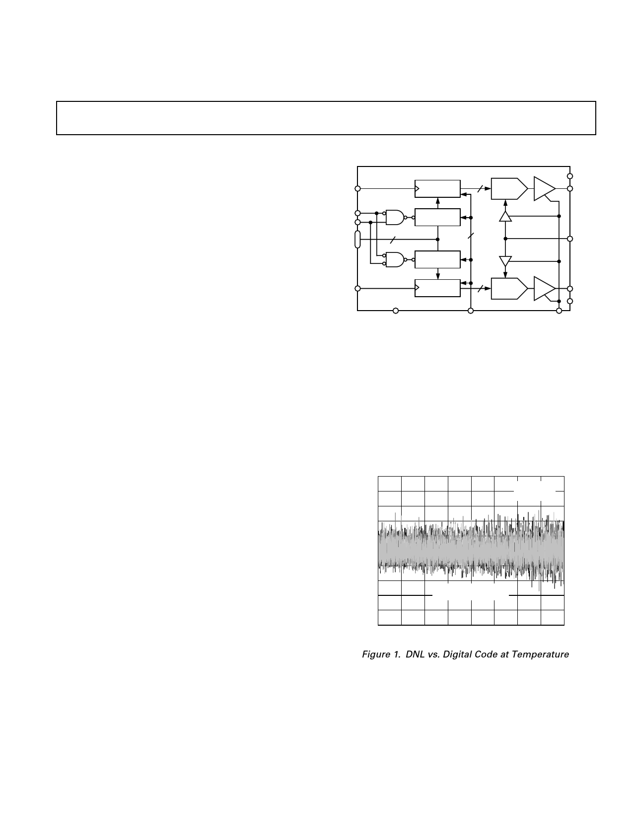
FUNCTIONAL BLOCK DIAGRAM
AD7396
LDA
CS
A/B
DATA
12
LDB
DACA
REGISTER
INPUTA
REGISTER
INPUTB
REGISTER
DACB
REGISTER
12 12-BIT
DACA
1
12 12-BIT
DACB
DGND
RS
VDD
VOUTA
VREF
VOUTB
AGND
SHDN
GENERAL DESCRIPTION
The AD7396/AD7397 series of dual, 12-bit and 10-bit voltage-
output digital-to-analog converters are designed to operate from
a single +3 V supply. Built using a CBCMOS process, these
monolithic DACs offer the user low cost and ease of use in
single supply +3 V systems. Operation is guaranteed over the
supply voltage range of +2.7 V to +5.5 V, making this device
ideal for battery operated applications.
A 12-bit wide data latch loads with a 45 ns write time allowing
interface to fast processors without wait states. The double
buffered input structure allows the user to load the input
registers one at a time, then a single load strobe tied to both
LDA+LDB inputs will simultaneously update both DAC out-
puts. LDA and LDB can also be independently activated to
immediately update their respective DAC registers. An address
input (A/B) decodes DACA or DACB when the chip select CS
input is strobed. Additionally, an asynchronous RS input sets
the output to zero-scale at power on or upon user demand.
Power shutdown to submicroamp levels is directly controlled by
the active low SHDN pin. While in the power shutdown state
register data can still be changed even though the output buffer
is in an open circuit state. Upon return to the normal operating
state the latest data loaded in the DAC register will establish the
output voltage.
Both parts are offered in the same pinout, allowing users to
select the amount of resolution appropriate for their applications
without circuit card changes.
The AD7396/AD7397 are specified for operation over the ex-
tended industrial (–40°C to +85°C) temperature range. The
AD7397AR is specified for the –40°C to +125°C automotive
temperature range. AD7396/AD7397s are available in plastic
DIP, and 24-lead SOIC packages. The AD7397ARU is avail-
able for ultracompact applications in a thin 1.1 mm height
TSSOP 24-lead package.
1.0
VDD = +3V
0.8 VREF = +2.5V
0.6
0.4
0.2
0.0
–0.2
–0.4
–0.6
TA = +25؇C, +85؇C, –55؇C
SUPERIMPOSED
–0.8
–1.0
0
512 1024 1536 2048 2560 3072 3584 4096
CODE – Decimal
Figure 1. DNL vs. Digital Code at Temperature
REV. 0
Information furnished by Analog Devices is believed to be accurate and
reliable. However, no responsibility is assumed by Analog Devices for its
use, nor for any infringements of patents or other rights of third parties
which may result from its use. No license is granted by implication or
otherwise under any patent or patent rights of Analog Devices.
One Technology Way, P.O. Box 9106, Norwood, MA 02062-9106, U.S.A.
Tel: 781/329-4700 World Wide Web Site: http://www.analog.com
Fax: 781/326-8703
© Analog Devices, Inc., 1998
1 page 
ABSOLUTE MAXIMUM RATINGS*
VDD to GND . . . . . . . . . . . . . . . . . . . . . . . . . . . . –0.3 V, +8 V
VREF to GND . . . . . . . . . . . . . . . . . . . . . . . . . . . . –0.3 V, VDD
Logic Inputs to GND . . . . . . . . . . . . . . . . . . . . . –0.3 V, +8 V
VOUT to GND . . . . . . . . . . . . . . . . . . . . . –0.3 V, VDD + 0.3 V
AGND to DGND . . . . . . . . . . . . . . . . . . . . . . . . –0.3 V, +2 V
IOUT Short Circuit to GND . . . . . . . . . . . . . . . . . . . . +50 mA
Package Power Dissipation . . . . . . . . . . . . . (TJ max – TA)/θJA
Thermal Resistance θJA
24-Lead Plastic DIP Package (N-24) . . . . . . . . . . +63°C/W
24-Lead SOIC Package (R-24) . . . . . . . . . . . . . . . +70°C/W
24-Lead Thin Shrink Surface Mount (RU-24) . . +143°C/W
AD7396/AD7397
Maximum Junction Temperature (TJ max) . . . . . . . . . +150°C
Operating Temperature Range . . . . . . . . . . . –40°C to +85°C
AD7397AN, AD7397AR Only . . . . . . . . –40°C to +125°C
Storage Temperature Range . . . . . . . . . . . . –65°C to +150°C
Lead Temperature
␣ ␣ N-24 (Soldering, 10 sec) . . . . . . . . . . . . . . . . . . . . . . +300°C
␣ ␣ R-24 (Vapor Phase, 60 sec) . . . . . . . . . . . . . . . . . . . . +215°C
␣ ␣ RU-24 (Infrared, 15 sec) . . . . . . . . . . . . . . . . . . . . . . +224°C
*Stresses above those listed under Absolute Maximum Ratings may cause perma-
nent damage to the device. This is a stress rating only; functional operation of the
device at these or any other conditions above those indicated in the operational
sections of this specification is not implied. Exposure to absolute maximum rating
conditions for extended periods may affect device reliability.
ORDERING GUIDE
Model
Res
(LSB)
Temperature
Ranges
Package
Descriptions
AD7396AN
AD7396AR
AD7397AN
AD7397AR
AD7397ARU
12
12
10
10
10
–40°C to +85°C
–40°C to +85°C
–40°C to +125°C
–40°C to +125°C
–40°C to +85°C
24-Lead P-DIP
24-Lead SOIC
24-Lead P-DIP
24-Lead SOIC
24-Lead Thin Shrink Small Outline Package (TSSOP)
The AD7396/AD7397 contains 1365 transistors. The die size measures 89 mil × 106 mil = 9434 sq mil.
Package
Options
N-24
R-24
N-24
R-24
RU-24
CAUTION
ESD (electrostatic discharge) sensitive device. Electrostatic charges as high as 4000 V readily
accumulate on the human body and test equipment and can discharge without detection.
Although the AD7396/AD7397 features proprietary ESD protection circuitry, permanent dam-
age may occur on devices subjected to high energy electrostatic discharges. Therefore, proper
ESD precautions are recommended to avoid performance degradation or loss of functionality.
WARNING!
ESD SENSITIVE DEVICE
REV. 0
–5–
5 Page 
AD7396/AD7397
allowing any new Input Register data updates to directly control
the DAC output voltages for single-buffered applications. For
doubled-buffered applications where both DAC outputs, VOUTA
and VOUTB, need to be changed simultaneously to a new value,
the two inputs, LDA and LDB, can be tied together and pulsed
active low in a synchronous manner.
RESET (RS) PIN
Forcing the asynchronous RS pin low will set the Input and
DAC registers to all zeros and the DAC output voltage will be
zero volts. The reset function is useful for setting the DAC
outputs to zero at power-up or after a power supply interrup-
tion. Test systems and motor controllers are two of many appli-
cations that benefit from powering up to a known state. The
external reset pulse can be generated by the microprocessor’s
power-on RESET signal, from the microprocessor, or by an
external resistor and capacitor. RESET has a Schmitt trigger
input which results in a clean reset function when using external
resistor/capacitor generated pulses. See Table I, Control-Logic
Truth.
POWER SHUTDOWN (SHDN)
Maximum power savings can be achieved by using the power
shutdown control function. This hardware-activated feature is
controlled by the active low input SHDN pin. This pin has a
Schmitt trigger input which helps to desensitize it to slowly
changing inputs. By placing a logic low on this pin the internal
consumption of the AD7397 or AD7397 is reduced to nanoamp
levels, guaranteed to 1.5 µA maximum over the operating tem-
perature range. If power is present at all times on the VDD pin
while in the shutdown mode, the internal DAC register will
retain the last programmed data value. This data will be used
when the part is returned to the normal active state by placing
the DAC back to its programmed voltage setting. Shutdown
recovery time measures 80 µs. In the shutdown state the DAC
output amplifier exhibits an open-circuit high-resistance state.
Any load connected will stabilize at its termination voltage. If
the power shutdown feature is not needed then the user should
tie the SHDN pin to the VDD voltage thereby disabling this
function.
UNIPOLAR OUTPUT OPERATION
This is the basic mode of operation for the AD7396. As shown
in Figure 29, the AD7396 has been designed to drive loads as
low as 5 kΩ in parallel with 100 pF. The code table for this
operation is shown in Table II.
0.01F
+2.7V TO +5.5V
R
VDD
AD7396
0.1F 10F
EXT
REF
VREF
DAC A
75k⍀
VOUTA
100pF
DAC B
16/14
C DIGITAL
75k⍀
VOUTB
100pF
DGND AGND
DIGITAL INTERFACE
CIRCUITRY OMITTED
FOR CLARITY.
Figure 29. Unipolar Output Operation
Table II. Unipolar Code Table
Hexadecimal
Number
In DAC Register
FFF
801
800
7FF
000
Decimal
Number
In DAC Register
4095
2049
2048
2047
0
Output
Voltage (V)
(VREF = 2.5 V)
2.4994
1.2506
1.2500
1.2494
0
The circuit can be configured with an external reference plus
power supply, or powered from a single dedicated regulator or
reference, depending on the application performance requirements.
BIPOLAR OUTPUT OPERATION
Although the AD7397 has been designed for single supply op-
eration, the output can easily be configured for bipolar opera-
tion. A typical circuit is shown in Figure 30. This circuit uses a
clean regulated +5 V supply for power, which also provides
the circuit’s reference voltage. Since the AD7397 output span
swings from ground to very near +5 V, it is necessary to choose
an external amplifier with a common-mode input voltage range
that extends to its positive supply rail. The micropower con-
sumption OP196 has been designed just for this purpose and
results in only 50 µA of maximum current consumption. Con-
nection of the equal-value 470 kΩ resistors results in a differen-
tial amplifier mode of operation with a voltage gain of two,
which produces a circuit output span of ten volts, that is,
–5 V to +5 V. As the AD7397 DAC is programmed from zero-
code 000H to midscale 200H to full-scale 3FFH, the circuit out-
put voltage VO is set at –5 V, 0 V and +5 V (–1 LSB). The
output voltage VO is coded in offset binary according to
Equation 3.
VOUT = [(D/512)–1] × 5
(4)
where D is the decimal code loaded in the AD7397 DAC regis-
ter. Note that the LSB step size is 10/1024 = 10 mV. This
circuit has been optimized for micropower consumption includ-
ing the 470 kΩ gain setting resistors, which should have low
temperature coefficients to maintain accuracy and matching
(preferably the same resistor material, such as metal film). If
better stability is required, the power supply could be substi-
tuted with a precision reference voltage such as the low dropout
REF195, which can easily supply the circuit’s 262 µA of current
and still provide additional power for the load connected to VO.
The micropower REF195 is guaranteed to source 10 mA output
drive current, but consumes only 50 µA internally. If higher
resolution is required, the AD7396 can be used with the addi-
tion of two more bits of data inserted into the software coding,
which would result in a 2.5 mV LSB step size. Table III shows
examples of nominal output voltages, VO, provided by the bipo-
lar operation circuit application.
REV. 0
–11–
11 Page | ||
| Páginas | Total 12 Páginas | |
| PDF Descargar | [ Datasheet AD7397.PDF ] | |
Hoja de datos destacado
| Número de pieza | Descripción | Fabricantes |
| AD7390 | 3 V Serial-Input Micropower 10-Bit and 12-Bit DACs | Analog Devices |
| AD7391 | +3 Volt Serial-Input Micropower 10-Bit & 12-Bit DACs | Analog Devices |
| AD7392 | +3 V/ Parallel Input Micropower 10- and 12-Bit DACs | Analog Devices |
| AD7393 | +3 V/ Parallel Input Micropower 10- and 12-Bit DACs | Analog Devices |
| Número de pieza | Descripción | Fabricantes |
| SLA6805M | High Voltage 3 phase Motor Driver IC. |
Sanken |
| SDC1742 | 12- and 14-Bit Hybrid Synchro / Resolver-to-Digital Converters. |
Analog Devices |
|
DataSheet.es es una pagina web que funciona como un repositorio de manuales o hoja de datos de muchos de los productos más populares, |
| DataSheet.es | 2020 | Privacy Policy | Contacto | Buscar |