|
|
|
PDF AD7339 Data sheet ( Hoja de datos )
| Número de pieza | AD7339 | |
| Descripción | 5 V Integrated High Speed ADC/Quad DAC System | |
| Fabricantes | Analog Devices | |
| Logotipo | ||
Hay una vista previa y un enlace de descarga de AD7339 (archivo pdf) en la parte inferior de esta página. Total 12 Páginas | ||
|
No Preview Available !
a
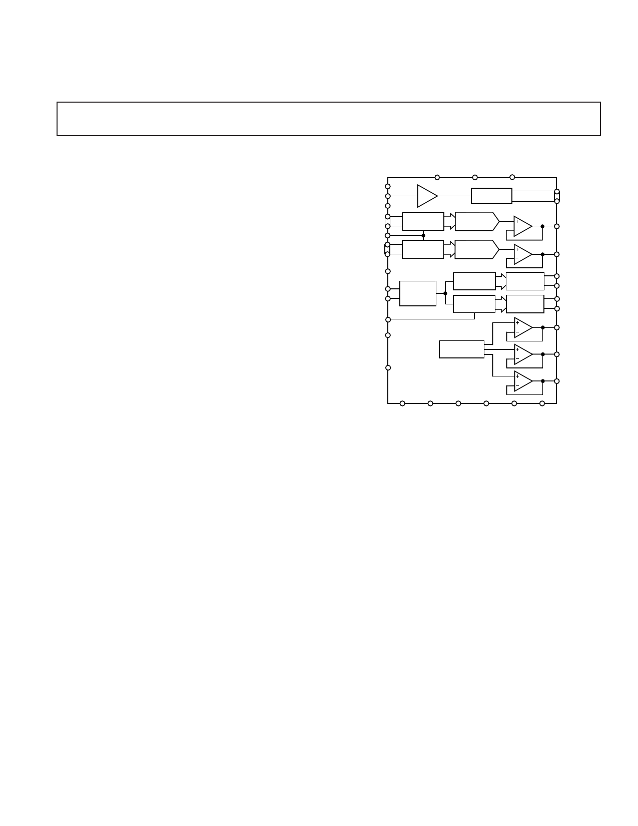
5 V Integrated High Speed ADC/Quad
DAC System
AD7339
FEATURES
8-Bit A/D Converter
Two 8-Bit D/A Converters
Two 8-Bit Serial D/A Converters
Single +5 V Supply Operation
On-Chip Reference
Power-Down Mode
52-Lead PQFP Package
GENERAL DESCRIPTION
The AD7339 is a composite IC that contains both DAC and
ADC functions. The device includes an 8-bit parallel A-to-D
converter. Two 8-bit parallel DACs are also included as are two
serial control DACs. These serial DACs are 8-bit DACs.
The AD7339, which operates with a single 5 V power supply,
has a bandgap reference on board with a nominal value of 2.5 V.
To reduce the power consumption of the part, each section,
except the reference, can be individually powered down when
not in use.
The AD7339 is available in a 52-lead PQFP package.
FUNCTIONAL BLOCK DIAGRAM
ADCPDB
AIN
ADCCLK
DA0
DA7
DACCLK
DB0
DB7
DACPDB
SDATA
SCLK
LATCH
SDACPDB
AVDD
DVDD1
DGND1
AGND1
T/H
DAC A
REGISTER
DAC B
REGISTER
ADC
PARALLEL
DAC A
PARALLEL
DAC B
SERIAL
CONTROL
LOGIC
DAC 0
REGISTER
DAC 1
REGISTER
SERIAL
DAC 0
SERIAL
DAC 1
2.5V
REFERENCE
AD7339
D0
D7
DACA
DACB
SDAC0F
SDAC0S
SDAC1F
SDAC1S
VREF
VREFA
VREFB
DVDD2 DVDD3 DGND2 DGND3 AGND2 AGND3
REV. 0
Information furnished by Analog Devices is believed to be accurate and
reliable. However, no responsibility is assumed by Analog Devices for its
use, nor for any infringements of patents or other rights of third parties
which may result from its use. No license is granted by implication or
otherwise under any patent or patent rights of Analog Devices.
One Technology Way, P.O. Box 9106, Norwood, MA 02062-9106, U.S.A.
Tel: 781/329-4700 World Wide Web Site: http://www.analog.com
Fax: 781/326-8703
© Analog Devices, Inc., 1997
1 page 
AD7339
ADCCLK
D0 – D7
SAMPLE N–2
N–3
SAMPLE N–1
t2
t3
t1
N–2
SAMPLE N
SAMPLE N+1
t4
N–1
t5
N
Figure 3. ADC Timing
SAMPLE N+2
N+1
DACCLK
DA0 – DA7
DB0 – DB7
DACA
DACB
t6
t7
DATA
t8
t11
t12
t9
DATA
t10
10%
90%
Figure 4. Parallel DACs Timing
SCLK
SDATA
LATCH
SDAC0S
SDAC1S
D1
t14
t13
t15
D0
t17
t16
D9(MSB)
t18
t19
Figure 5. Serial DACs Timing
D8
10%
D7
REV. 0
–5–
5 Page 
AD7339
TERMINOLOGY
Differential Nonlinearity
The difference between the measured and the ideal 1 LSB change
between any two adjacent codes in the ADC or DACs. A speci-
fied Differential Nonlinearity of ± 1 LSB max over the operating
temperature range ensures monotonicity.
Integral Nonlinearity
The maximum deviation of any code from a straight line passing
through the endpoints of the transfer function. The endpoints
of the transfer function are zero scale, a point 0.5 LSB below the
first code transition (000 . . . 00 to 000 . . . 01) and full scale, a
point 0.5 LSB above the last code transition (111 . . . 10 to
111 . . . 11). The error is expressed in LSBs.
Signal to (Noise + Distortion)
Signal to (Noise + Distortion) is measured signal-to-noise at the
output of the ADC. The signal is the rms magnitude of the
fundamental. Noise is the rms sum of all nonfundamental sig-
nals up to half the sampling frequency (FS/2) excluding dc.
Signal to (Noise + Distortion) is dependent on the number of
quantization levels used in the digitization process; the more
levels, the smaller the quantization noise. The theoretical signal
to (Noise + Distortion) ratio for a sine wave signal is given by
Signal to (Noise + Distortion) = (6.02N + 1.76) dB
where N is the number of bits. Thus for an ideal 8-bit converter,
Signal to (Noise + Distortion) is 49.92 dB.
ADC
Effective Number of Bits (ENOB)
Signal to (Noise + Distortion) is expressed in dBs; rewriting the
Signal to (Noise + Distortion) formula, it is possible to get a
measure of performance expressed in effective number of bits.
The effective number of bits for a device can be calculated di-
rectly from its measured Signal to (Noise + Distortion) value.
ENOB = (SNR – 1.76)/6.02
where SNR is the Signal to (Noise + Distortion).
Zero Input Offset Error
This is the offset error in the ADC when the analog input is
zero. Ideally, the digital output should equal 100 . . . 00. The
offset error is the deviation from the ideal output code. The
offset error is expressed in LSBs.
Intermodulation Distortion
With inputs consisting of sine waves at two frequencies, fa and
fb, any active device with nonlinearities will create distortion
products, of order (m + n), at sum and difference frequencies
of mfa ± nfb, where m, n = 0, 1, 2, 3, . . .. Intermodulation
terms are those for which m or n is not equal to zero. For the
AD7339, the Intermodulation Distortion is the level to which
the second and third intermodulation terms are suppressed
below a full scale output signal level, the second order terms
being (fa + fb) and (fa – fb) while the third order terms are
(2fa + fb), (2fa – fb), (fa + 2fb) and (fa – 2fb).
Error Rate
The rate at which A-to-D conversion errors occur.
DACS
Bipolar Zero Offset Error
The deviation between the measured output voltage and the
bias voltage (VREFA or VREFB, depending on which DAC is
being tested) when the DAC is loaded with code 100 . . . 00
after gain error has been adjusted out.
Gain Error
A measure of the output error between an ideal DAC and the
actual device output with all 1s loaded after offset error has been
adjusted out.
Update Rate
The rate at which the DACs can be loaded with new data. The
parallel DACs have an update rate of 2.304 MHz while the
serial DACs have an update rate of 256/10 kHz maximum.
Gain Matching Between DACs
The matching between the analog output amplitudes of the
parallel DACs when the same digital word is written to each
DAC.
Crosstalk
The ratio of the amplitude of a full-scale signal appearing on
one channel to the amplitude of the same signal which couples
onto another channel. Crosstalk is expressed in dBs.
Output Harmonic Content
When the digital word is converted to analog form, harmonics
will also be generated. The Output Harmonic Content specifies
the amount by which these harmonics are attenuated relative to
the fundamental frequency. With the parallel DACs, a full sine
wave of frequency 0 kHz to 128 kHz is input. The resulting
analog output is evaluated and the amount by which the
harmonics in the frequency band 0 MHz to 1.1152 MHz are
attenuated is measured relative to the magnitude of the fun-
damental output signal.
REV. 0
–11–
11 Page | ||
| Páginas | Total 12 Páginas | |
| PDF Descargar | [ Datasheet AD7339.PDF ] | |
Hoja de datos destacado
| Número de pieza | Descripción | Fabricantes |
| AD7330 | Low Quiescent Current Low Dropout CMOS Voltage Regulator | Advanced Corporation Limited |
| AD73311 | Low Cost/ Low Power CMOS General Purpose Analog Front End | Analog Devices |
| AD73311L | Low Cost/ Low Power CMOS General Purpose Analog Front End | Analog Devices |
| AD73322 | Low Cost/ Low Power CMOS General-Purpose Dual Analog Front End | Analog Devices |
| Número de pieza | Descripción | Fabricantes |
| SLA6805M | High Voltage 3 phase Motor Driver IC. |
Sanken |
| SDC1742 | 12- and 14-Bit Hybrid Synchro / Resolver-to-Digital Converters. |
Analog Devices |
|
DataSheet.es es una pagina web que funciona como un repositorio de manuales o hoja de datos de muchos de los productos más populares, |
| DataSheet.es | 2020 | Privacy Policy | Contacto | Buscar |