|
|
|
PDF AD676 Data sheet ( Hoja de datos )
| Número de pieza | AD676 | |
| Descripción | 16-Bit 100 kSPS Sampling ADC | |
| Fabricantes | Analog Devices | |
| Logotipo | ||
Hay una vista previa y un enlace de descarga de AD676 (archivo pdf) en la parte inferior de esta página. Total 16 Páginas | ||
|
No Preview Available !
a
16-Bit 100 kSPS
Sampling ADC
FEATURES
Autocalibrating
On-Chip Sample-Hold Function
Parallel Output Format
16 Bits No Missing Codes
؎1 LSB INL
–97 dB THD
90 dB S/(N+D)
1 MHz Full Power Bandwidth
AD676
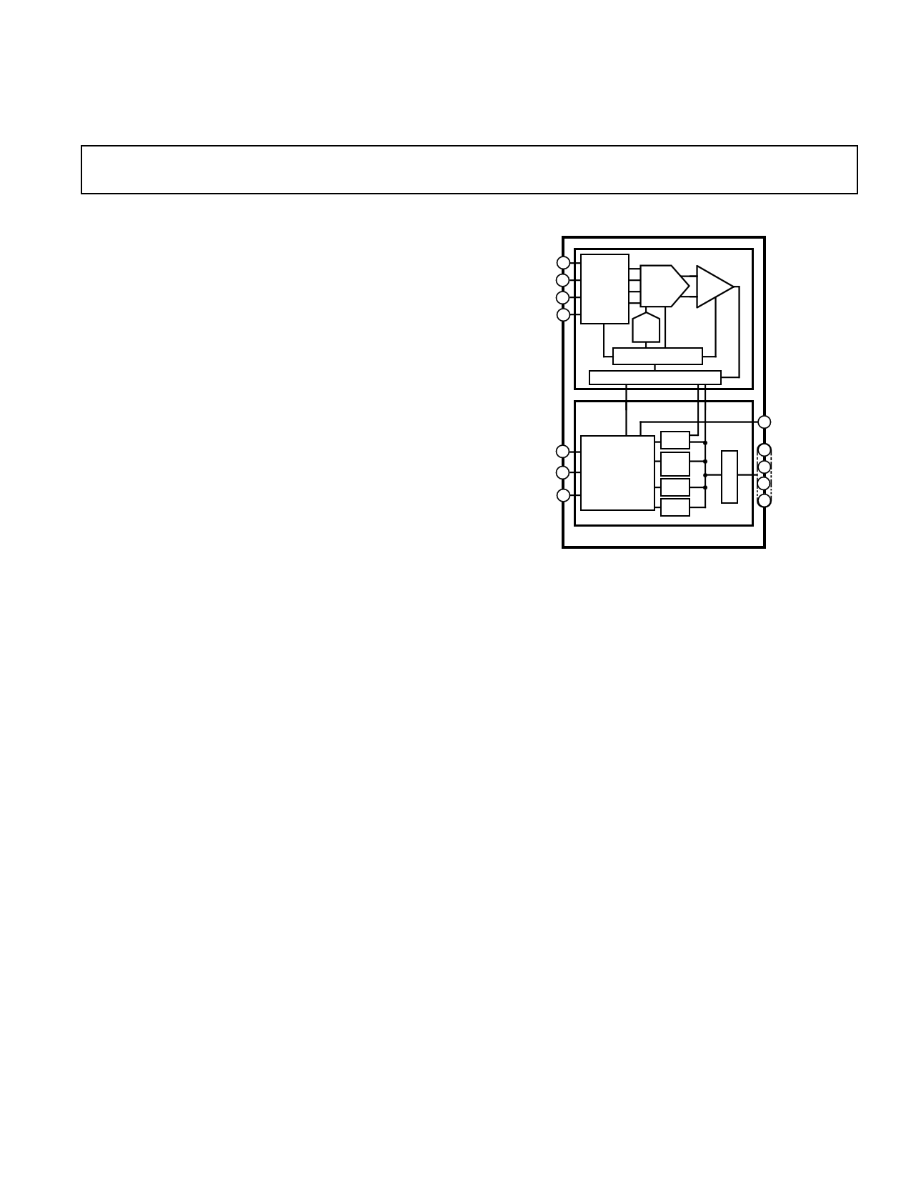
FUNCTIONAL BLOCK DIAGRAM
VIN 15
AGND SENSE 14
VREF 16
AGND 13
INPUT
BUFFERS
16-BIT
DAC
CAL
DAC
ANALOG
CHIP
COMP
LOGIC & TIMING
LEVEL TRANSLATORS
PRODUCT DESCRIPTION
The AD676 is a multipurpose 16-bit parallel output analog-to-
digital converter which utilizes a switched-capacitor/charge
redistribution architecture to achieve a 100 kSPS conversion
rate (10 µs total conversion time). Overall performance is opti-
mized by digitally correcting internal nonlinearities through
on-chip autocalibration.
The AD676 circuitry is segmented onto two monolithic chips—
a digital control chip fabricated on Analog Devices DSP CMOS
process and an analog ADC chip fabricated on our BiMOS II
process. Both chips are contained in a single package.
The AD676 is specified for ac (or “dynamic”) parameters such
as S/(N+D) Ratio, THD and IMD which are important in sig-
nal processing applications. In addition, dc parameters are
specified which are important in measurement applications.
DIGITAL
CHIP
CAL 8
SAMPLE 9
CLK 10
MICRO-CODED
CONTROLLER
SAR
PAT
GEN
ALU
RAM
7 BUSY
1
L
A6
T BIT 1 – BIT 16
C 19
H 28
AD676
The AD676 operates from +5 V and ± 12 V supplies and typi-
cally consumes 360 mW during conversion. The digital supply
(VDD) is separated from the analog supplies (VCC, VEE) for re-
duced digital crosstalk. An analog ground sense is provided for
the analog input. Separate analog and digital grounds are also
provided.
The AD676 is available in a 28-pin plastic DIP or 28-pin side-
brazed ceramic package. A serial-output version, the AD677, is
available in a 16-pin 300 mil wide ceramic or plastic package.
REV. A
Information furnished by Analog Devices is believed to be accurate and
reliable. However, no responsibility is assumed by Analog Devices for its
use, nor for any infringements of patents or other rights of third parties
which may result from its use. No license is granted by implication or
otherwise under any patent or patent rights of Analog Devices.
One Technology Way, P.O. Box 9106, Norwood, MA 02062-9106, U.S.A.
Tel: 617/329-4700
Fax: 617/326-8703
1 page 
AD676
ORDERING GUIDE
Model
Temperature Range1
S/(N+D)
Package
Max INL Package Description Option2
AD676JD
AD676KD
AD676AD
AD676BD
0°C to +70°C
0°C to +70°C
–40°C to +85°C
–40°C to +85°C
85 dB
87 dB
85 dB
87 dB
± 1.5 LSB
± 1.5 LSB
Ceramic 28-Pin DIP
Ceramic 28-Pin DIP
Ceramic 28-Pin DIP
Ceramic 28-Pin DIP
D-28
D-28
D-28
D-28
NOTES
1For details on grade and package offerings screened in accordance with MIL-STD-883, refer to the AD676/883 data sheet.
2D = Ceramic DIP.
ABSOLUTE MAXIMUM RATINGS*
VCC to VEE . . . . . . . . . . . . . . . . . . . . . . . . . . –0.3 V to +26.4 V
VDD to DGND . . . . . . . . . . . . . . . . . . . . . . . . . –0.3 V to +7 V
VCC to AGND . . . . . . . . . . . . . . . . . . . . . . . . –0.3 V to +18 V
VEE to AGND . . . . . . . . . . . . . . . . . . . . . . . . –18 V to +0.3 V
AGND to DGND . . . . . . . . . . . . . . . . . . . . . . . . . . . . ± 0.3 V
Digital Inputs to DGND . . . . . . . . . . . . . . . . . . 0 V to +5.5 V
Analog Inputs, VREF to AGND
. . . . . . . . . . . . . . . . . . . . . . . (VCC + 0.3 V) to (VEE – 0.3 V)
Soldering . . . . . . . . . . . . . . . . . . . . . . . . . . . . . +300°C, 10 sec
Storage Temperature . . . . . . . . . . . . . . . . . . –65°C to +150°C
*Stresses greater than those listed under “Absolute Maximum Ratings” may cause
permanent damage to the device. This is a stress rating only and functional
operation of the device at these or any other conditions above those indicated in
the operational section of this specification is not implied. Exposure to absolute
maximum rating conditions for extended periods may affect device reliability.
CAUTION
The AD676 features input protection circuitry consisting of large “distributed” diodes and
polysilicon series resistors to dissipate both high energy discharges (Human Body Model) and fast,
low energy pulses (Charged Device Model). Per Method 3015.2 of MIL-STD-883C, the AD676
has been classified as a Category 1 Device.
Proper ESD precautions are strongly recommended to avoid functional damage or performance
degradation. Charges as high as 4000 volts readily accumulate on the human body and test
equipment, and discharge without detection. Unused devices must be stored in conductive foam
or shunts, and the foam discharged to the destination socket before devices are removed. For further
information on ESD Precaution. Refer to Analog Devices’ ESD Prevention Manual.
WARNING!
ESD SENSITIVE DEVICE
REV. A
–5–
5 Page 
Using AGND SENSE to remotely sense the ground potential of
the signal source can be useful if the signal has to be carried
some distance to the A/D converter. Since all IC ground cur-
rents have to return to the power supply and no ground leads
are free from resistance and inductance, there are always some
voltage differences from one ground point in a system to
another.
Over distance this voltage difference can easily amount to sev-
eral LSBs (in a 10 V input span, 16-bit system each LSB is
about 0.15 mV). This would directly corrupt the A/D input sig-
nal if the A/D measures its input with respect to power ground
(AGND) as shown in Figure 5a. To solve this problem the
AD676 offers an AGND SENSE pin. Figure 5b shows how the
AGND SENSE can be used to eliminate the problem in Figure
5a. Figure 5b also shows how the signal wires should be
shielded in a noisy environment to avoid capacitive coupling. If
inductive (magnetic) coupling is expected to be dominant such
as where motors are present, twisted-pair wires should be used
instead.
The digital ground pin is the reference point for all of the digital
signals that operate the AD676. This pin should be connected
to the digital common point in the system. As Figure 4 illus-
trated, the analog and digital grounds should be connected to-
gether at one point in the system, preferably at the AD676.
SOURCE
VS
AD676
VIN
∆V AGND
GROUND LEAD
IGROUND > 0
TO POWER
SUPPLY GND
Figure 5a. Input to the A/D Is Corrupted by IR Drop in
Ground Leads: VIN = VS + ∆V
SOURCE
VS
SHIELDED CABLE
AD676
VIN
AGND
SENSE
AGND
GROUND LEAD
IGROUND > 0
TO POWER
SUPPLY GND
Figure 5b. AGND SENSE Eliminates the Problem in
Figure 5a.
AD676
VOLTAGE REFERENCE
The AD676 requires the use of an external voltage reference.
The input voltage range is determined by the value of the refer-
ence voltage; in general, a reference voltage of n volts allows an
input range of ± n volts. The AD676 is specified for both 10 V
and 5.0 V references. A 10 V reference will typically require
support circuitry operated from ± 15 V supplies; a 5.0 V refer-
ence may be used with ± 12 V supplies. Signal-to-noise perfor-
mance is increased proportionately with input signal range. In
the presence of a fixed amount of system noise, increasing the
LSB size (which results from increasing the reference voltage)
will increase the effective S/(N+D) performance. Figure 12
illustrates S/(N+D) as a function of reference voltage. In
contrast, INL will be optimal at lower reference voltage values
(such as 5 V) due to capacitor nonlinearity at higher voltage
values.
During a conversion, the switched capacitor array of the AD676
presents a dynamically changing current load at the voltage ref-
erence as the successive-approximation algorithm cycles through
various choices of capacitor weighting. (See the following sec-
tion “Analog Input” for a detailed discussion of the VREF input
characteristics.) The output impedance of the reference circuitry
must be low so that the output voltage will remain sufficiently
constant as the current drive changes. In some applications, this
may require that the output of the voltage reference be buffered
by an amplifier with low impedance at relatively high frequen-
cies. In choosing a voltage reference, consideration should be
made for selecting one with low noise. A capacitor connected
between REF IN and AGND will reduce the demands on the
reference by decreasing the magnitude of high frequency com-
ponents required to be sourced by the reference.
Figures 6 and 7 represent typical design approaches.
+12V
CN
1.0µF
2
VIN
8 AD586 6
4
10µF
16 VREF
+
13 AGND
AD676
Figure 6.
Figure 6 shows a voltage reference circuit featuring the 5 V out-
put AD586. The AD586 is a low cost reference which utilizes a
buried Zener architecture to provide low noise and drift. Over
the 0°C to +70°C range, the AD586L grade exhibits less than
2.25 mV output change from its initial value at +25°C. A noise-
reduction capacitor, CN, reduces the broadband noise of the
REV. A
–11–
11 Page | ||
| Páginas | Total 16 Páginas | |
| PDF Descargar | [ Datasheet AD676.PDF ] | |
Hoja de datos destacado
| Número de pieza | Descripción | Fabricantes |
| AD670 | Low Cost Signal Conditioning 8-Bit ADC | Analog Devices |
| AD671 | Monolithic 12-Bit 2 MHz A/D Converter | Analog Devices |
| AD673 | 8-Bit A/D Converter | Analog Devices |
| AD674B | Complete 12-Bit A/D Converters | Analog Devices |
| Número de pieza | Descripción | Fabricantes |
| SLA6805M | High Voltage 3 phase Motor Driver IC. |
Sanken |
| SDC1742 | 12- and 14-Bit Hybrid Synchro / Resolver-to-Digital Converters. |
Analog Devices |
|
DataSheet.es es una pagina web que funciona como un repositorio de manuales o hoja de datos de muchos de los productos más populares, |
| DataSheet.es | 2020 | Privacy Policy | Contacto | Buscar |