|
|
|
PDF AD667 Data sheet ( Hoja de datos )
| Número de pieza | AD667 | |
| Descripción | Microprocessor-Compatible 12-Bit D/A Converter | |
| Fabricantes | Analog Devices | |
| Logotipo | ||
Hay una vista previa y un enlace de descarga de AD667 (archivo pdf) en la parte inferior de esta página. Total 8 Páginas | ||
|
No Preview Available !
a
Microprocessor-Compatible
12-Bit D/A Converter
AD667*
FEATURES
Complete 12-Bit D/A Function
Double-Buffered Latch
On Chip Output Amplifier
High Stability Buried Zener Reference
Single Chip Construction
Monotonicity Guaranteed Over Temperature
Linearity Guaranteed Over Temperature: 1/2 LSB max
Settling Time: 3 s max to 0.01%
Guaranteed for Operation with ؎12 V or ؎15 V
Supplies
Low Power: 300 mW Including Reference
TTL/5 V CMOS Compatible Logic Inputs
Low Logic Input Currents
MIL-STD-883 Compliant Versions Available
PRODUCT DESCRIPTION
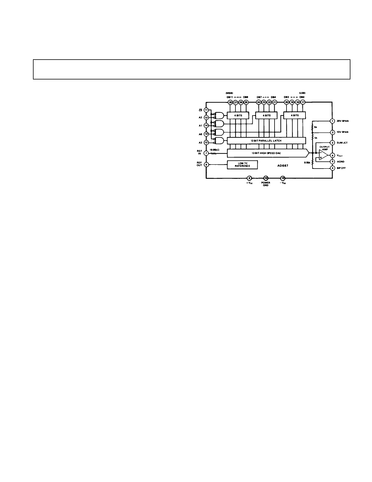
The AD667 is a complete voltage output 12-bit digital-to-analog
converter including a high stability buried Zener voltage refer-
ence and double-buffered input latch on a single chip. The
converter uses 12 precision high speed bipolar current steering
switches and a laser trimmed thin-film resistor network to pro-
vide fast settling time and high accuracy.
Microprocessor compatibility is achieved by the on-chip double-
buffered latch. The design of the input latch allows direct inter-
face to 4-, 8-, 12-, or 16-bit buses. The 12 bits of data from the
first rank of latches can then be transferred to the second rank,
avoiding generation of spurious analog output values. The latch
responds to strobe pulses as short as 100 ns, allowing use with
the fastest available microprocessors.
The functional completeness and high performance in the
AD667 results from a combination of advanced switch design,
high speed bipolar manufacturing process, and the proven laser
wafer-trimming (LWT) technology. The AD667 is trimmed at
the wafer level and is specified to ± 1/4 LSB maximum linearity
error (K, B grades) at +25°C and ± 1/2 LSB over the full operat-
ing temperature range.
The subsurface (buried) Zener diode on the chip provides a low
noise voltage reference which has long-term stability and tem-
perature drift characteristics comparable to the best discrete ref-
erence diodes. The laser trimming process which provides the
excellent linearity, is also used to trim the absolute value of the
reference as well as its temperature coefficient. The AD667 is
thus well suited for wide temperature range performance with
± 1/2 LSB maximum linearity error and guaranteed monotonic-
ity over the full temperature range. Typical full-scale gain TC is
5 ppm/°C.
*Protected by Patent Numbers 3,803,590; 3,890,611; 3,932,863; 3,978,473;
4,020,486; and others pending.
REV. A
Information furnished by Analog Devices is believed to be accurate and
reliable. However, no responsibility is assumed by Analog Devices for its
use, nor for any infringements of patents or other rights of third parties
which may result from its use. No license is granted by implication or
otherwise under any patent or patent rights of Analog Devices.
FUNCTIONAL BLOCK DIAGRAM
The AD667 is available in five performance grades. The
AD667J and K are specified for use over the 0°C to +70°C tem-
perature range and are available in a 28-pin molded plastic DIP
(N) or PLCC (P) package. The AD667S grade is specified for
the –55°C to +125°C range and is available in the ceramic DIP
(D) or LCC (E) package. The AD667A and B are specified for
use over the –25°C to +85°C temperature range and are avail-
able in a 28-pin hermetically sealed ceramic DIP (D) package.
PRODUCT HIGHLIGHTS
1. The AD667 is a complete voltage output DAC with voltage
reference and digital latches on a single IC chip.
2. The double-buffered latch structure permits direct interface
to 4-, 8-, 12-, or 16-bit data buses. All logic inputs are TTL
or 5 volt CMOS compatible.
3. The internal buried Zener reference is laser-trimmed to 10.00
volts with a ± 1% maximum error. The reference voltage is
also available for external application.
4. The gain setting and bipolar offset resistors are matched to
the internal ladder network to guarantee a low gain tempera-
ture coefficient and are laser-trimmed for minimum full-scale
and bipolar offset errors.
5. The precision high speed current steering switch and on-board
high speed output amplifier settle within 1/2 LSB for a 10 V
full-scale transition in 2.0 µs as when properly compensated.
6. The AD667 is available in versions compliant with MIL-
STD-883. Refer to the Analog Devices Military Products
Databook or current AD667/883B data sheet for detailed
specifications.
One Technology Way, P.O. Box 9106, Norwood, MA 02062-9106, U.S.A.
Tel: 617/329-4700
Fax: 617/326-8703
1 page 
ANALOG CIRCUIT CONNECTIONS
Internal scaling resistors provided in the AD667 may be connected
to produce bipolar output voltage ranges of ±10, ±5 or ±2.5 V or
unipolar output voltage ranges of 0 V to +5 V or 0 V to +10 V.
Gain and offset drift are minimized in the AD667 because of the
thermal tracking of the scaling resistors with other device com-
ponents. Connections for various output voltage ranges are
shown in Table I.
AD667
Figure 3. ±5 V Bipolar Voltage Output
Figure 1. Output Amplifier Voltage Range Scaling Circuit
UNIPOLAR CONFIGURATION (Figure 2)
This configuration will provide a unipolar 0 volt to +10 volt out-
put range. In this mode, the bipolar offset terminal, Pin 4, should
be grounded if not used for trimming.
Figure 2. 0 V to +10 V Unipolar Voltage Output
STEP I . . . ZERO ADJUST
Turn all bits OFF and adjust zero trimmer R1, until the output
reads 0.000 volts (1 LSB = 2.44 mV). In most cases this trim is
not needed, and Pin 4 should be connected to Pin 5.
STEP II . . . GAIN ADJUST
Turn all bits ON and adjust 100 Ω gain trimmer R2, until the
output is 9.9976 volts. (Full scale is adjusted to 1 LSB less than
nominal full scale of 10.000 volts.)
BIPOLAR CONFIGURATION (Figure 3)
This configuration will provide a bipolar output voltage from
–5.000 to +4.9976 volts, with positive full scale occurring with
all bits ON (all 1s).
STEP I . . . OFFSET ADJUST
Turn OFF all bits. Adjust 100 Ω trimmer R1 to give –5.000
volts output.
STEP II . . . GAIN ADJUST
Turn ON all bits. Adjust 100 Ω gain trimmer R2 to give a read-
ing of +4.9976 volts.
INTERNAL/EXTERNAL REFERENCE USE
The AD667 has an internal low noise buried Zener diode refer-
ence which is trimmed for absolute accuracy and temperature
coefficient. This reference is buffered and optimized for use in a
high speed DAC and will give long-term stability equal or superior
to the best discrete Zener reference diodes. The performance of
the AD667 is specified with the internal reference driving the
DAC since all trimming and testing (especially for full-scale
error and bipolar offset) is done in this configuration.
The internal reference has sufficient buffering to drive external
circuitry in addition to the reference currents required for the
DAC (typically 0. 5 mA to Ref In and 1.0 mA to Bipolar Off-
set). A minimum of 0.1 mA is available for driving external
loads. The AD667 reference output should be buffered with an
external op amp if it is required to supply more than 0.1 mA
output current. The reference is typically trimmed to ± 0.2%,
then tested and guaranteed to ± 1.0% max error. The tempera-
ture coefficient is comparable to that of the full-scale TC for a
particular grade.
If an external reference is used (10.000 V, for example), addi-
tional trim range must be provided, since the internal reference
has a tolerance of ± 1%, and the AD667 full-scale and bipolar
offset are both trimmed with the internal reference. The gain
and offset trim resistors give about ± 0.25% adjustment range,
which is sufficient for the AD667 when used with the internal
reference.
It is also possible to use external references other than 10 volts.
The recommended range of reference voltage is from +8 to
+11 volts, which allows both 8.192 V and 10.24 V ranges to be
used. The AD667 is optimized for fixed-reference applications.
If the reference voltage is expected to vary over a wide range in a
particular application, a CMOS multiplying DAC is a better
choice.
Reduced values of reference voltage will also permit the ± 12
volt ± 5% power supply requirement to be relaxed to ± 12 volts
± 10%.
It is not recommended that the AD667 be used with external
feedback resistors to modify the scale factor. The internal resis-
tors are trimmed to ratio-match and temperature-track the other
resistors on the chip, even though their absolute tolerances are
± 20%, and absolute temperature coefficients are approximately
–50 ppm/°C. If external resistors are used, a wide trim range
(± 20%) will be needed and temperature drift will be increased
to reflect the mismatch between the temperature coefficients of
the internal and external resistors.
REV. A
–5–
5 Page | ||
| Páginas | Total 8 Páginas | |
| PDF Descargar | [ Datasheet AD667.PDF ] | |
Hoja de datos destacado
| Número de pieza | Descripción | Fabricantes |
| AD660 | Monolithic 16-Bit Serial/Byte DACPORT | Analog Devices |
| AD6600 | Dual Channel/ Gain-Ranging ADC with RSSI | Analog Devices |
| AD6620 | 65 MSPS Digital Receive Signal Processor | Analog Devices |
| AD6622 | Four-Channel/ 75 MSPS Digital Transmit Signal Processor TSP | Analog Devices |
| Número de pieza | Descripción | Fabricantes |
| SLA6805M | High Voltage 3 phase Motor Driver IC. |
Sanken |
| SDC1742 | 12- and 14-Bit Hybrid Synchro / Resolver-to-Digital Converters. |
Analog Devices |
|
DataSheet.es es una pagina web que funciona como un repositorio de manuales o hoja de datos de muchos de los productos más populares, |
| DataSheet.es | 2020 | Privacy Policy | Contacto | Buscar |