|
|
|
PDF AD636 Data sheet ( Hoja de datos )
| Número de pieza | AD636 | |
| Descripción | Low Level/ True RMS-to-DC Converter | |
| Fabricantes | Analog Devices | |
| Logotipo | ||
Hay una vista previa y un enlace de descarga de AD636 (archivo pdf) en la parte inferior de esta página. Total 8 Páginas | ||
|
No Preview Available !
a
Low Level,
True RMS-to-DC Converter
AD636
FEATURES
True RMS-to-DC Conversion
200 mV Full Scale
Laser-Trimmed to High Accuracy
0.5% Max Error (AD636K)
1.0% Max Error (AD636J)
Wide Response Capability:
Computes RMS of AC and DC Signals
1 MHz –3 dB Bandwidth: V RMS >100 mV
Signal Crest Factor of 6 for 0.5% Error
dB Output with 50 dB Range
Low Power: 800 A Quiescent Current
Single or Dual Supply Operation
Monolithic Integrated Circuit
Low Cost
Available in Chip Form
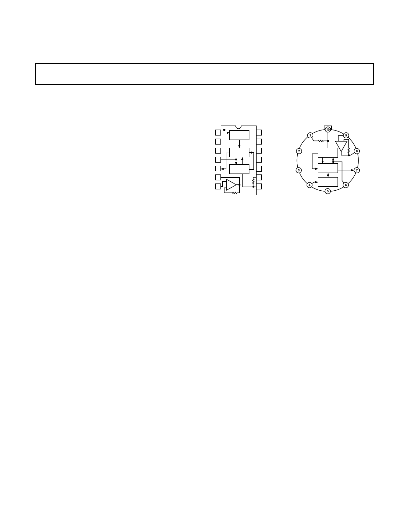
PIN CONNECTIONS &
FUNCTIONAL BLOCK DIAGRAM
IOUT
VIN 1
ABSOLUTE
VALUE
NC 2 AD636
–VS 3
CAV 4
SQUARER
DIVIDER
dB 5
CURRENT
MIRROR
BUF OUT 6
BUF IN 7
+
BUF
– 10k⍀
10k⍀
14 +VS
13 NC
12 NC
11 NC
COMMON
RL BUF IN
10k⍀
AD636
+–
BUF
BUF OUT
CURRENT
MIRROR
10k⍀
10 COMMON
9 RL
8 IOUT
+VS
VIN
SQUARER
DIVIDER
ABSOLUTE
VALUE
dB
CAV
NC = NO CONNECT
–VS
PRODUCT DESCRIPTION
The AD636 is a low power monolithic IC which performs true
rms-to-dc conversion on low level signals. It offers performance
which is comparable or superior to that of hybrid and modular
converters costing much more. The AD636 is specified for a
signal range of 0 mV to 200 mV rms. Crest factors up to 6 can
be accommodated with less than 0.5% additional error, allowing
accurate measurement of complex input waveforms.
The low power supply current requirement of the AD636, typi-
cally 800 µA, allows it to be used in battery-powered portable
instruments. A wide range of power supplies can be used, from
± 2.5 V to ±16.5 V or a single +5 V to +24 V supply. The input
and output terminals are fully protected; the input signal can
exceed the power supply with no damage to the device (allowing
the presence of input signals in the absence of supply voltage)
and the output buffer amplifier is short-circuit protected.
The AD636 includes an auxiliary dB output. This signal is
derived from an internal circuit point which represents the loga-
rithm of the rms output. The 0 dB reference level is set by an
externally supplied current and can be selected by the user
to correspond to any input level from 0 dBm (774.6 mV) to
–20 dBm (77.46 mV). Frequency response ranges from 1.2 MHz
at a 0 dBm level to over 10 kHz at –50 dBm.
The AD636 is designed for ease of use. The device is factory-
trimmed at the wafer level for input and output offset, positive
and negative waveform symmetry (dc reversal error), and full-
scale accuracy at 200 mV rms. Thus no external trims are re-
quired to achieve full-rated accuracy.
AD636 is available in two accuracy grades; the AD636J total
error of ± 0.5 mV ± 0.06% of reading, and the AD636K
is accurate within ± 0.2 mV to ± 0.3% of reading. Both versions
are specified for the 0°C to +70°C temperature range, and are
offered in either a hermetically sealed 14-pin DIP or a 10-lead
TO-100 metal can. Chips are also available.
PRODUCT HIGHLIGHTS
1. The AD636 computes the true root-mean-square of a com-
plex ac (or ac plus dc) input signal and gives an equivalent dc
output level. The true rms value of a waveform is a more
useful quantity than the average rectified value since it is a
measure of the power in the signal. The rms value of an
ac-coupled signal is also its standard deviation.
2. The 200 millivolt full-scale range of the AD636 is compatible
with many popular display-oriented analog-to-digital con-
verters. The low power supply current requirement permits
use in battery powered hand-held instruments.
3. The only external component required to perform measure-
ments to the fully specified accuracy is the averaging capaci-
tor. The value of this capacitor can be selected for the desired
trade-off of low frequency accuracy, ripple, and settling time.
4. The on-chip buffer amplifier can be used to buffer either the
input or the output. Used as an input buffer, it provides
accurate performance from standard 10 MΩ input attenua-
tors. As an output buffer, it can supply up to 5 milliamps of
output current.
5. The AD636 will operate over a wide range of power supply
voltages, including single +5 V to +24 V or split ± 2.5 V to
± 16.5 V sources. A standard 9 V battery will provide several
hundred hours of continuous operation.
REV. B
Information furnished by Analog Devices is believed to be accurate and
reliable. However, no responsibility is assumed by Analog Devices for its
use, nor for any infringements of patents or other rights of third parties
which may result from its use. No license is granted by implication or
otherwise under any patent or patent rights of Analog Devices.
One Technology Way, P.O. Box 9106, Norwood, MA 02062-9106, U.S.A.
Tel: 781/329-4700 World Wide Web Site: http://www.analog.com
Fax: 781/326-8703
© Analog Devices, Inc., 1999
1 page 
AD636
100 100
10 10
1.0 1.0
VALUES FOR CAV AND
1% SETTLING TIME FOR
0.1 STATED % OF READING
AVERAGING ERROR*
ACCURACY ؎20% DUE TO
COMPONENT TOLERANCE
0.1
*% dc ERROR + % RIPPLE (PEAK)
0.01
1 10 100 1k
0.01
10k 100k
INPUT FREQUENCY – Hz
Figure 5. Error/Settling Time Graph for Use with the
Standard rms Connection
The primary disadvantage in using a large CAV to remove ripple
is that the settling time for a step change in input level is in-
creased proportionately. Figure 5 shows the relationship be-
tween CAV and 1% settling time is 115 milliseconds for each
microfarad of CAV. The settling time is twice as great for de-
creasing signals as for increasing signals (the values in Figure 5
are for decreasing signals). Settling time also increases for low
signal levels, as shown in Figure 6.
VIN
–VS
+–
CAV
1 ABSOLUTE
VALUE
2 AD636
3 SQUARER
DIVIDER
4
5
CURRENT
MIRROR
6+
10k⍀
7 B–UF
10k⍀
14
13
12
11
10
9
8
+VS
(FOR SINGLE POLE, SHORT Rx,
REMOVE C3)
+
C2 –
Rx
10k⍀
–
C3 +
Vrms OUT
Figure 7. 2 Pole ‘’Post’’ Filter
10
p-p RIPPLE
(ONE POLE)
CAV = 1F
C2 = 4.7F
p-p RIPPLE
CAV = 1F (FIG 1)
1 DC ERROR
CAV = 1F
(ALL FILTERS)
p-p RIPPLE
(TWO POLE)
10.0 CAV = 1F, C2 = C3 = 4.7F
0.1
10 100 1k 10k
7.5 FREQUENCY – Hz
Figure 8. Performance Features of Various Filter Types
5.0
RMS MEASUREMENTS
AD636 PRINCIPLE OF OPERATION
2.5 The AD636 embodies an implicit solution of the rms equation
1.0
0
1mV
10mV
100mV
rms INPUT LEVEL
Figure 6. Settling Time vs. Input Level
1V
A better method for reducing output ripple is the use of a
“post-filter.” Figure 7 shows a suggested circuit. If a single pole
filter is used (C3 removed, RX shorted), and C2 is approxi-
mately 5 times the value of CAV, the ripple is reduced as shown
in Figure 8, and settling time is increased. For example, with
CAV = 1 µF and C2 = 4.7 µF, the ripple for a 60 Hz input is re-
duced from 10% of reading to approximately 0.3% of reading.
The settling time, however, is increased by approximately a
factor of 3. The values of CAV and C2 can therefore be reduced
to permit faster settling times while still providing substantial
ripple reduction.
The two-pole post-filter uses an active filter stage to provide
even greater ripple reduction without substantially increasing
the settling times over a circuit with a one-pole filter. The values
of CAV, C2, and C3 can then be reduced to allow extremely fast
settling times for a constant amount of ripple. Caution should
be exercised in choosing the value of CAV, since the dc error is
dependent upon this value and is independent of the post filter.
For a more detailed explanation of these topics refer to the
RMS-to-DC Conversion Application Guide, 2nd Edition, available
that overcomes the dynamic range as well as other limitations
inherent in a straightforward computation of rms. The actual
computation performed by the AD636 follows the equation:
V
rms
=
Avg. VVIrNm2s
Figure 9 is a simplified schematic of the AD636; it is subdivided
into four major sections: absolute value circuit (active rectifier),
squarer/divider, current mirror, and buffer amplifier. The input
voltage, VIN, which can be ac or dc, is converted to a unipolar
current I1, by the active rectifier A1, A2. I1 drives one input of
the squarer/divider, which has the transfer function:
I4 =
I12
I3
The output current, I4, of the squarer/divider drives the current
mirror through a low-pass filter formed by R1 and the externally
connected capacitor, CAV. If the R1, CAV time constant is much
greater than the longest period of the input signal, then I4 is
effectively averaged. The current mirror returns a current I3,
which equals Avg. [I4], back to the squarer/divider to complete
the implicit rms computation. Thus:
I4
=
Avg.
I12
I4
=
I1
rms
from Analog Devices.
REV. B
–5–
5 Page | ||
| Páginas | Total 8 Páginas | |
| PDF Descargar | [ Datasheet AD636.PDF ] | |
Hoja de datos destacado
| Número de pieza | Descripción | Fabricantes |
| AD630 | Balanced Modulator/Demodulator | Analog Devices |
| AD6311 | 1/8- to 1/16 Duty VFD Controller/Driver | Anachip |
| AD6312 | 1/4- to 1/11 Duty VFD Controller/Driver | Anachip |
| AD6315 | 1/4- to 1/12 Duty VFD Controller/Driver | Anachip |
| Número de pieza | Descripción | Fabricantes |
| SLA6805M | High Voltage 3 phase Motor Driver IC. |
Sanken |
| SDC1742 | 12- and 14-Bit Hybrid Synchro / Resolver-to-Digital Converters. |
Analog Devices |
|
DataSheet.es es una pagina web que funciona como un repositorio de manuales o hoja de datos de muchos de los productos más populares, |
| DataSheet.es | 2020 | Privacy Policy | Contacto | Buscar |