|
|
|
PDF AD606 Data sheet ( Hoja de datos )
| Número de pieza | AD606 | |
| Descripción | 80 dB Demodulating Logarithmic Amplifier | |
| Fabricantes | Analog Devices | |
| Logotipo | ||
Hay una vista previa y un enlace de descarga de AD606 (archivo pdf) en la parte inferior de esta página. Total 13 Páginas | ||
|
No Preview Available !
a 50 MHz, 80 dB Demodulating
Logarithmic Amplifier with Limiter Output
AD606
FEATURES
Logarithmic Amplifier Performance
–75 dBm to +5 dBm Dynamic Range
≤1.5 nV/√Hz Input Noise
Usable to >50 MHz
37.5 mV/dB Voltage Output
On-Chip Low-Pass Output Filter
Limiter Performance
؎1 dB Output Flatness over 80 dB Range
؎3؇ Phase Stability at 10.7 MHz over 80 dB Range
Adjustable Output Amplitude
Low Power
+5 V Single Supply Operation
65 mW Typical Power Consumption
CMOS-Compatible Power-Down to 325 W typ
<5 s Enable/Disable Time
APPLICATIONS
Ultrasound and Sonar Processing
Phase-Stable Limiting Amplifier to 100 MHz
Received Signal Strength Indicator (RSSI)
Wide Range Signal and Power Measurement
PRODUCT DESCRIPTION
The AD606 is a complete, monolithic logarithmic amplifier
using a 9-stage “successive-detection” technique. It provides
both logarithmic and limited outputs. The logarithmic output is
from a three-pole post-demodulation low-pass filter and provides
a loadable output voltage of +0.1 V dc to +4 V dc. The logarith-
mic scaling is such that the output is +0.5 V for a sinusoidal
input of –75 dBm and +3.5 V at an input of +5 dBm; over this
range the logarithmic linearity is typically within ± 0.4 dB. All
scaling parameters are proportional to the supply voltage.
The AD606 can operate above and below these limits, with
reduced linearity, to provide as much as 90 dB of conversion
range. A second low-pass filter automatically nulls the input
offset of the first stage down to the submicrovolt level. Adding
external capacitors to both filters allows operation at input fre-
quencies as low as a few hertz.
The AD606’s limiter output provides a hard-limited signal
output as a differential current of ± 1.2 mA from open-collector
outputs. In a typical application, both of these outputs are
loaded by 200 Ω resistors to provide a voltage gain of more than
90 dB from the input. Transition times are 1.5 ns, and the
phase is stable to within ± 3° at 10.7 MHz for signals from
–75 dBm to +5 dBm.
The logarithmic amplifier operates from a single +5 V supply
and typically consumes 65 mW. It is enabled by a CMOS logic
level voltage input, with a response time of <5 µs. When dis-
abled, the standby power is reduced to <1 mW within 5 µs.
The AD606J is specified for the commercial temperature range
of 0°C to +70°C and is available in 16-lead plastic DIPs or
SOICs. Consult the factory for other packages and temperature
ranges.
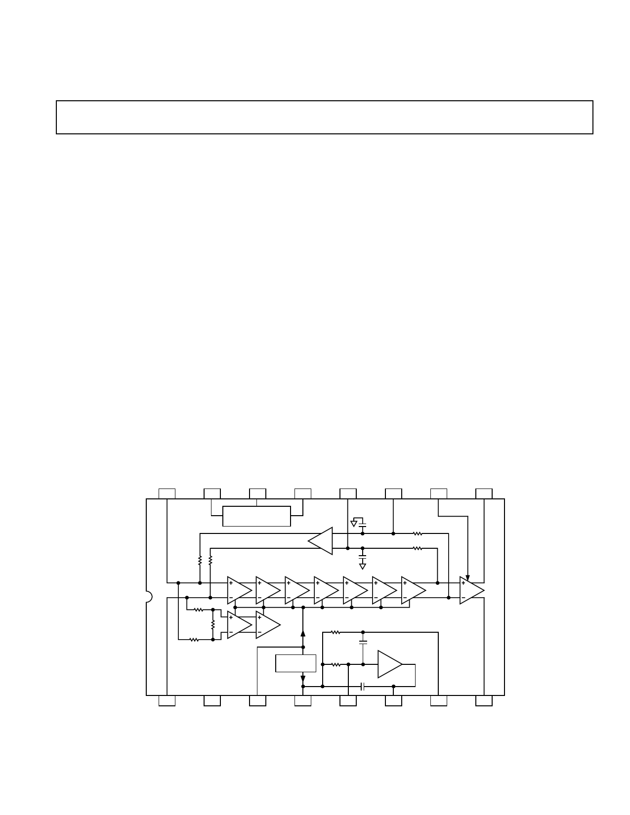
FUNCTIONAL BLOCK DIAGRAM
INHI
16
COMM
15
PRUP
14
VPOS
13
FIL1
12
FIL2
11
LADJ
10
LMHI
9
REFERENCE
AND POWER-UP
30k⍀
30k⍀
30pF
360k⍀
X1
30pF
360k⍀
OFFSET-NULL
LOW-PASS FILTER
1.5k⍀
250⍀
1.5k⍀
HIGH-END
DETECTORS
AD606
MAIN SIGNAL PATH
11.15dB/STAGE
12A/dB
ONE-POLE
FILTER
2A/dB
9.375k⍀
9.375k⍀
2pF TWO-POLE
SALLEN-KEY
FILTER
X2
2pF
FINAL
LIMITER
REV. B
1
INLO
2
COMM
3
ISUM
4
ILOG
Information furnished by Analog Devices is believed to be accurate and
reliable. However, no responsibility is assumed by Analog Devices for its
use, nor for any infringements of patents or other rights of third parties
which may result from its use. No license is granted by implication or
otherwise under any patent or patent rights of Analog Devices.
5
BFIN
6
VLOG
7
OPCM
8
LMLO
One Technology Way, P.O. Box 9106, Norwood, MA 02062-9106, U.S.A.
Tel: 781/329-4700 World Wide Web Site: http://www.analog.com
Fax: 781/326-8703
© Analog Devices, Inc., 1999
1 page 
AD606
INPUT LEVEL CONVENTIONS
RF logarithmic amplifiers usually have their input specified in
“dBm,” meaning “decibels with respect to 1 mW.” Unfortu-
nately, this is not precise for several reasons.
1. Log amps respond not to power but to voltage. In this re-
spect, it would be less ambiguous to use “dBV” (decibels
referred to 1 V) as the input metric. Also, power is dependent
on the rms (root mean-square) value of the signal, while log
amps are not inherently rms responding.
2. The response of a demodulating log amp depends on the
waveform. Convention assumes that the input is sinusoidal.
However, the AD606 is capable of accurately handling any
input waveform, including ac voltages, pulses and square
waves, Gaussian noise, and so on. See the AD640 data sheet,
which covers the effect of waveform on logarithmic intercept,
for more information.
3. The impedance in which the specified power is measured is
not always stated. In the log amp context it is invariably
assumed to be 50 Ω. Thus, 0 dBm means “1 mW rms in 50 Ω,”
and corresponds to an rms voltage of (1 mW × 50 Ω), or
224 mV.
Popular convention requires the use of dBm to simplify the
comparison of log amp specifications. Unless otherwise stated,
sinusoidal inputs expressed as dBm in 50 Ω are used to specify
the performance of the AD606 throughout this data sheet. We
will also show the corresponding rms voltages where it helps to
clarify the specification. Noise levels will likewise be given in
dBm; the response to Gaussian noise is 0.5 dB higher than for a
sinusoidal input of the same rms value.
Note that dynamic range, being a simple ratio, is always speci-
fied simply as “dB”, and the slope of the logarithmic transfer
function is correctly specified as “mV/dB,” NOT as “mV/dBm.”
LOGARITHMIC SLOPE AND INTERCEPT
A generalized logarithmic amplifier having an input voltage VIN
and output voltage VLOG must satisfy a transfer function of the
form
VLOG = VY log10 (VIN /VX )
where, in the case of the AD606, the voltage VIN is the differ-
ence between the voltages on pins INHI and INLO, and the
voltage VLOG is that measured at the output pin VLOG. VY and
VX are fixed voltages that determine the slope and intercept of
the logarithmic amplifier, respectively. These parameters are
inherent in the design of a particular logarithmic amplifier,
although may be adjustable, as in the AD606. When VIN = VX,
the logarithmic argument is one, hence the logarithm is zero. VX
is, therefore, called the logarithmic intercept voltage because the
output voltage VLOG crosses zero for this input. The slope volt-
age VY is can also be interpreted as the “volts per decade” when
using base-10 logarithms as shown here.
results in an alternating input voltage being transformed into a
quasi-dc (rectified and filtered) output voltage.
The single supply nature of the AD606 results in common-mode
level of the inputs INHI and INLO being at about +2.5 V (us-
ing the recommended +5 V supply). In normal ac operation,
this bias level is developed internally and the input signal is
coupled in through dc blocking capacitors. Any residual dc
offset voltage in the first stage limits the logarithmic accuracy for
small inputs. In ac operation, this offset is automatically and
continuously nulled via a feedback path from the last stage, pro-
vided that the pins INHI and INLO are not shorted together, as
would be the case if transformer coupling were used for the signal.
While any logarithmic amplifier must eventually conform to the
basic equation shown above, which, with appropriate elabora-
tion, can also fully account for the effect of the signal waveform
on the effective intercept,1 it is more convenient in RF applica-
tions to use a simpler expression. This simplification results
from first, assuming that the input is always sinusoidal, and
second, using a decibel representation for the input level. The
standard representation of RF levels is (incorrectly, in a log amp
context) in terms of power, specifically, decibels above 1 milli-
watt (dBm) with a presumed impedance level of 50 Ω. That
being the case, we can rewrite the transfer function as
VLOG = VY (PIN – PX )
where it must be understood that PIN means the sinusoidal input
power level in a 50 Ω system, expressed in dBm, and PX is the
intercept, also expressed in dBm. In this case, PIN and PX are
simple, dimensionless numbers. (PX is sometimes called the
“logarithmic offset,” for reasons which are obvious from the
above equation.) VY is still defined as the logarithmic slope,
usually specified as so many millivolts per decibel, or mV/dB.
In the case of the AD606, the slope voltage, VY, is nominally
750 mV when operating at VPOS = 5 V. This can also be ex-
pressed as 37.5 mV/dB or 750 mV/decade; thus, the 80 dB
range equates to 3 V. Figure 1 shows the transfer function of the
AD606. The slope is closely proportional to VPOS, and can more
generally be stated as VY = 0.15 × VPOS. Thus, in those applica-
tions where the scaling must be independent of supply voltage,
this must be stabilized to the required accuracy. In applications
where the output is applied to an A/D converter, the reference
4
3.5
3
2.5
SLOPE = 37.5mV/dB
2
1.5
Note carefully that VLOG and VLOG in the above paragraph
(and elsewhere in this data sheet) are different. The first is a
voltage; the second is a pin designation.
This equation suggests that the input VIN is a dc quantity, and,
if VX is positive, that VIN must likewise be positive, since the
logarithm of a negative number has no simple meaning. In fact,
in the AD606, the response is independent of the sign of VIN
because of the particular way in which the circuit is built. This
is part of the demodulating nature of the amplifier, which
1
0.5
INTERCEPT
AT –88.33dBm
0
–100
–80
–60
–40
–20
0
+20
INPUT SIGNAL – dBm
Figure 1. Nominal Transfer Function
1See, for example, the AD640 data sheet, which is published in Section 3 of
the Special Linear Reference Manual or Section 9.3 of the 1992 Amplifier
Applications Guide.
–4– REV. B
5 Page 
8/30/99 9 AM
AD606–Typical Performance Characteristics
0.5
–0.5
–1.5
–2.5
–3.5
70MHz
45MHz
10.7MHz
–4.5
–5.5
–6.5
–80 –70 –60 –50 –40 –30 –20 –10 0 20
INPUT LEVEL – dBm
Figure 10. Normalized Limiter
Amplitude Response vs. Input Level
at 10.7 MHz, 45 MHz and 70 MHz
5
0 45MHz
–5
10.7MHz
70MHz
–10
–15
–20
–25
–80
–60 –40 –20
0
INPUT LEVEL – dBm
20
Figure 11. Normalized Limiter
Phase Response vs. Input Level at
10.7 MHz, 45 MHz, and 70 MHz
14
12
10
8
6
4
2
0
0 0.5 1 1.5 2 2.5 3 3.5 4 4.5 5
PRUP VOLTAGE – Volts
Figure 12. Supply Current vs. PRUP
Voltage at +25°C
4.5
TA = +25؇C
4
3.5 VS = 5.5V
3
2.5
2 VS = 5V
1.5
1 VS = 4.5V
0.5
0
–80 –60 –40 –20
0
INPUT POWER – dBm
10
Figure 13. VLOG Plotted vs. Input
Level at 10.7 MHz as a Function of
Power Supply Voltage
4
3
2
1 TA = –25؇C
TA = +25؇C
0
–1
TA = +70؇C
–2
–3
–4
–80
–60 –40
–20
0
INPUT AMPLITUDE – dBm
10
Figure 14. Logarithmic Conform-
ance as a Function of Input Level at
10.7 MHz at –25°C, +25°C, and
+70°C
5
4
3
2
1
0
–1
–2
–3
–4
–5
–80
TA = –25؇C
TA = +25؇C
TA = +70؇C
–60 –40 –20
0
INPUT AMPLITUDE – dBm
10
Figure 15. Logarithmic Conform-
ance as a Function of Input Level at
45 MHz at –25°C, +25°C, and +70°C
Figure 16. Limiter Response at
Onset of 10.7 MHz Modulated Pulse
at –75 dBm Using 200 pF Input
Coupling Capacitors
Figure 17. VLOG Response to a
10.7 MHz CW Signal Modulated by
a 25 µs Wide Pulse with a 25 kHz
Repetition Rate Using 200 pF Input
Coupling Capacitors. The Input Sig-
nal Goes from +5 dBm to –75 dBm
in 20 dB Steps.
Figure 18. Limiter Response at
Onset of 70 MHz Modulated Pulse
at –55 dBm Using 200 pF Input
Coupling Capacitors
–10–
REV. B
11 Page | ||
| Páginas | Total 13 Páginas | |
| PDF Descargar | [ Datasheet AD606.PDF ] | |
Hoja de datos destacado
| Número de pieza | Descripción | Fabricantes |
| AD600 | Dual/ Low Noise/ Wideband Variable Gain Amplifiers | Analog Devices |
| AD602 | Dual/ Low Noise/ Wideband Variable Gain Amplifiers | Analog Devices |
| AD6025GP | Fan | ADDA |
| AD603 | Variable Gain Amplifier | Analog Devices |
| Número de pieza | Descripción | Fabricantes |
| SLA6805M | High Voltage 3 phase Motor Driver IC. |
Sanken |
| SDC1742 | 12- and 14-Bit Hybrid Synchro / Resolver-to-Digital Converters. |
Analog Devices |
|
DataSheet.es es una pagina web que funciona como un repositorio de manuales o hoja de datos de muchos de los productos más populares, |
| DataSheet.es | 2020 | Privacy Policy | Contacto | Buscar |