|
|
|
PDF AD598 Data sheet ( Hoja de datos )
| Número de pieza | AD598 | |
| Descripción | LVDT Signal Conditioner | |
| Fabricantes | Analog Devices | |
| Logotipo | ||
Hay una vista previa y un enlace de descarga de AD598 (archivo pdf) en la parte inferior de esta página. Total 16 Páginas | ||
|
No Preview Available !
a
LVDT Signal
Conditioner
AD598
FEATURES
Single Chip Solution, Contains Internal Oscillator and
Voltage Reference
No Adjustments Required
Insensitive to Transducer Null Voltage
Insensitive to Primary to Secondary Phase Shifts
DC Output Proportional to Position
20 Hz to 20 kHz Frequency Range
Single or Dual Supply Operation
Unipolar or Bipolar Output
Will Operate a Remote LVDT at Up to 300 Feet
Position Output Can Drive Up to 1000 Feet of Cable
Will Also Interface to an RVDT
Outstanding Performance
Linearity: 0.05% of FS max
Output Voltage: ؎11 V min
Gain Drift: 50 ppm/؇C of FS max
Offset Drift: 50 ppm/؇C of FS max
PRODUCT DESCRIPTION
The AD598 is a complete, monolithic Linear Variable Differen-
tial Transformer (LVDT) signal conditioning subsystem. It is
used in conjunction with LVDTs to convert transducer mechan-
ical position to a unipolar or bipolar dc voltage with a high
degree of accuracy and repeatability. All circuit functions are
included on the chip. With the addition of a few external passive
components to set frequency and gain, the AD598 converts the
raw LVDT secondary output to a scaled dc signal. The device
can also be used with RVDT transducers.
The AD598 contains a low distortion sine wave oscillator to
drive the LVDT primary. The LVDT secondary output consists
of two sine waves that drive the AD598 directly. The AD598
operates upon the two signals, dividing their difference by their
sum, producing a scaled unipolar or bipolar dc output.
The AD598 uses a unique ratiometric architecture (patent pend-
ing) to eliminate several of the disadvantages associated with
traditional approaches to LVDT interfacing. The benefits of this
new circuit are: no adjustments are necessary, transformer null
voltage and primary to secondary phase shift does not affect sys-
tem accuracy, temperature stability is improved, and transducer
interchangeability is improved.
The AD598 is available in two performance grades:
Grade Temperature Range Package
AD598JR 0°C to +70°C
AD598AD –40°C to +85°C
20-Pin Small Outline (SOIC)
20-Pin Ceramic DIP
It is also available processed to MIL-STD-883B, for the military
range of –55°C to +125°C.
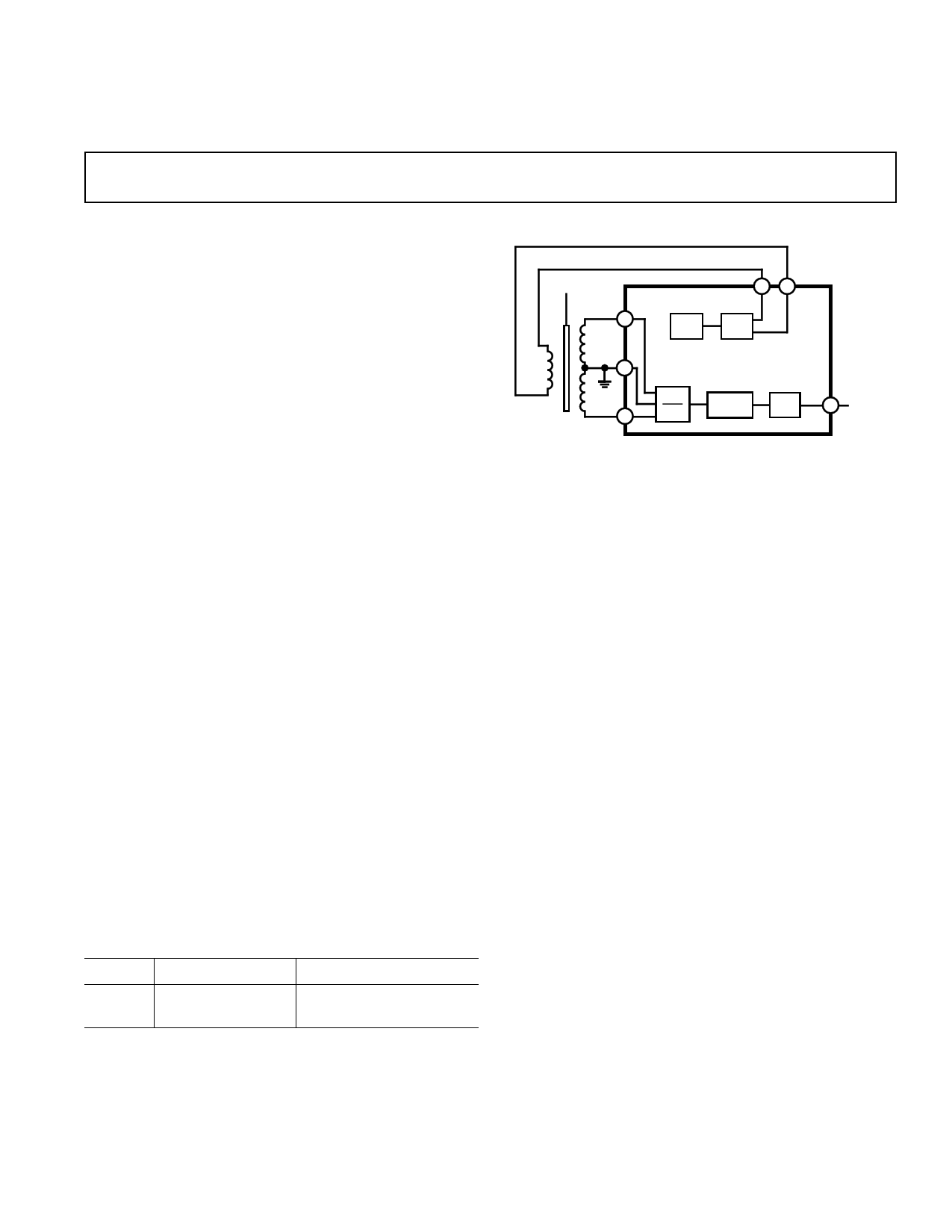
FUNCTIONAL BLOCK DIAGRAM
EXCITATION (CARRIER)
VA
11
32
OSC
AMP
17
LVDT
10
VB
AD598
A–B
A+B
FILTER AMP
16 VOUT
PRODUCT HIGHLIGHTS
1. The AD598 offers a monolithic solution to LVDT and
RVDT signal conditioning problems; few extra passive com-
ponents are required to complete the conversion from me-
chanical position to dc voltage and no adjustments are
required.
2. The AD598 can be used with many different types of
LVDTs because the circuit accommodates a wide range of
input and output voltages and frequencies; the AD598 can
drive an LVDT primary with up to 24 V rms and accept sec-
ondary input levels as low as 100 mV rms.
3. The 20 Hz to 20 kHz LVDT excitation frequency is deter-
mined by a single external capacitor. The AD598 input sig-
nal need not be synchronous with the LVDT primary drive.
This means that an external primary excitation, such as the
400 Hz power mains in aircraft, can be used.
4. The AD598 uses a ratiometric decoding scheme such that
primary to secondary phase shifts and transducer null voltage
have absolutely no effect on overall circuit performance.
5. Multiple LVDTs can be driven by a single AD598, either in
series or parallel as long as power dissipation limits are not
exceeded. The excitation output is thermally protected.
6. The AD598 may be used in telemetry applications or in hos-
tile environments where the interface electronics may be re-
mote from the LVDT. The AD598 can drive an LVDT at
the end of 300 feet of cable, since the circuit is not affected
by phase shifts or absolute signal magnitudes. The position
output can drive as much as 1000 feet of cable.
7. The AD598 may be used as a loop integrator in the design of
simple electromechanical servo loops.
REV. A
Information furnished by Analog Devices is believed to be accurate and
reliable. However, no responsibility is assumed by Analog Devices for its
use, nor for any infringements of patents or other rights of third parties
which may result from its use. No license is granted by implication or
otherwise under any patent or patent rights of Analog Devices.
One Technology Way, P.O. Box 9106, Norwood, MA 02062-9106, U.S.A.
Tel: 617/329-4700
Fax: 617/326-8703
1 page 
AD598
a voltage proportional to position. This technique uses the pri-
mary excitation voltage as a phase reference to determine the
polarity of the output voltage. There are a number of problems
associated with this technique such as (1) producing a constant
amplitude, constant frequency excitation signal, (2) compensating
for LVDT primary to secondary phase shifts, and (3) compen-
sating for these shifts as a function of temperature and frequency.
The AD598 eliminates all of these problems. The AD598 does
not require a constant amplitude because it works on the ratio of
the difference and sum of the LVDT output signals. A constant
frequency signal is not necessary because the inputs are rectified
and only the sine wave carrier magnitude is processed. There is
no sensitivity to phase shift between the primary excitation and
the LVDT outputs because synchronous detection is not em-
ployed. The ratiometric principle upon which the AD598 oper-
ates requires that the sum of the LVDT secondary voltages
remains constant with LVDT stroke length. Although LVDT
manufacturers generally do not specify the relationship between
VA+VB and stroke length, it is recognized that some LVDTs do
not meet this requirement. In these cases a nonlinearity will
result. However, the majority of available LVDTs do in fact
meet these requirements.
The AD598 utilizes a special decoder circuit. Referring to the
block diagram and Figure 6 below, an implicit analog comput-
ing loop is employed. After rectification, the A and B signals are
multiplied by complementary duty cycle signals, d and (I–d)
respectively. The difference of these processed signals is inte-
grated and sampled by a comparator. It is the output of this
comparator that defines the original duty cycle, d, which is fed
back to the multipliers.
As shown in Figure 6, the input to the integrator is [(A+B)d]B.
Since the integrator input is forced to 0, the duty cycle d =
B/(A+B).
The output comparator which produces d = B/(A+B) also con-
trols an output amplifier driven by a reference current. Duty
cycle signals d and (1–d) perform separate modulations on the
reference current as shown in Figure 6, which are summed. The
summed current, which is the output current, is IREF × (1–2d).
Since d = B/(A+B), by substitution the output current equals
IREF × (A–B)/(A+B). This output current is then filtered and
converted to a voltage since it is forced to flow through the scal-
ing resistor R2 such that:
VOUT = IREF × ( A – B ) / (A + B ) × R2
CONNECTING THE AD598
The AD598 can easily be connected for dual or single supply
operation as shown in Figures 7 and 12. The following general
design procedures demonstrate how external component values
are selected and can be used for any LVDT which meets AD598
input/output criteria.
Parameters which are set with external passive components in-
clude: excitation frequency and amplitude, AD598 system
bandwidth, and the scale factor (V/inch). Additionally, there are
optional features, offset null adjustment, filtering, and signal in-
tegration which can be used by adding external components.
INPUT
V TO I
COMP
±1
A
FILT
d
∑
0<d<1
BINARY SIGNAL
d - DUTY CYCLE
INTEG
COMP
INPUT
V TO I
COMP
±1
(A+B) d–B
B
FILT
1–d
dq B
A+B
BANDGAP
REFERENCE
IREF
1–d
IREF
q
A–B
A+B
d∑
FILT
∑
INTEG
VOLTS
OUTPUT
REV. A
RTO
OFFSET
V TO I
VOUT
= RSCALE
x I REF
x
A–B
A+B
Figure 6. Block Diagram of Decoder
–5–
5 Page 
AD598
–V
MASTER
+V
1 –VS
2 EXC 1
+VS 20
OFFSET 1 19
15k
3 EXC 2
OFFSET 2 18
4 LEV 1
5 LEV 2
0.015µF
6 FREQ 1
SIG REF 17
82.5kΩ
SIG OUT 16
FEEDBACK 15
7 FREQ 2 OUT FILT 14
8 B1 FILT
A1 FILT 13
9 B2 FILT
A2 FILT 12
0.1µF
10 VB AD598
VA 11
0.33µF
0.1µF
–V
15k
1 –VS
SLAVE 1
+V
+VS 20
2 EXC 1
OFFSET 1 19
3 EXC 2
OFFSET 2 18
4 LEV 1
5 LEV 2
SIG REF 17
82.5kΩ
SIG OUT 16
6 FREQ 1 FEEDBACK 15
0.1µF
7 FREQ 2
8 B1 FILT
9 B2 FILT
OUT FILT 14
A1 FILT 13
A2 FILT 12
0.33µF
0.1µF
10 VB AD598 VA 11
15k
–V
15k
1 –VS
SLAVE 2
+V
+VS 20
2 EXC 1
OFFSET 1 19
3 EXC 2
OFFSET 2 18
4 LEV 1
5 LEV 2
SIG REF 17
82.5kΩ
SIG OUT 16
6 FREQ 1 FEEDBACK 15
0.1µF
7 FREQ 2
8 B1 FILT
9 B2 FILT
OUT FILT 14
A1 FILT 13
A2 FILT 12
0.33µF
0.1µF
10 VB AD598 VA 11
SCHAEVITZ E 100 LVDT
MECHANICAL POSITION INPUT
SCHAEVITZ E 100 LVDT
MECHANICAL POSITION INPUT
Figure 21. Multiple LVDTs—Synchronous Operation
SCHAEVITZ E 100 LVDT
MECHANICAL POSITION INPUT
HIGH RESOLUTION POSITION-TO-FREQUENCY
CIRCUIT
In the circuit shown in Figure 22, the AD598 is combined with
an AD652 voltage-to-frequency (V/F) converter to produce an
effective, simple data converter which can make high resolution
measurements.
This circuit transfers the signal from the LVDT to the V/F con-
verter in the form of a current, thus eliminating the errors nor-
mally caused by the offset voltage of the V/F converter. The V/F
converter offset voltage is normally the largest source of error in
such circuits. The analog input signal to the AD652 is converted
to digital frequency output pulses which can be counted by
simple digital means.
This circuit is particularly useful if there is a large degree of
mechanical vibration (hum) on the position to be measured.
The hum may be completely rejected by counting the digital fre-
quency pulses over a gate time (fixed period) equal to a multiple
of the hum period. For the effects of the hum to be completely
rejected, the hum must be a periodic signal.
–Vs
0.1µF
GND
+Vs
0.1µF
1 –VS
2 EXC 1
+VS 20
OFFSET 1 19
3 EXC 2
OFFSET 2 18
4 LEV 1
SIG REF 17
5 LEV 2
0.015µF
SIG OUT 16
6 FREQ 1 FEEDBACK 15
7 FREQ 2 OUT FILT 14
8 B1 FILT
A1 FILT 13
9 B2 FILT
A2 FILT 12
0.1µF
10 VB AD598
VA 11
0.33µF
0.1µF
0.02µF
1 +VS
2 TRIM
3 TRIM
AD652
SYNCHRONOUS
VOLTAGE TO
FREQUENCY
CONVERTER
COMP REF 16
COMP“+” 15
COMP“–” 14
4 OP AMP OUT
ANALOG GND 13
5 OP AMP “–”
6 OP AMP “+”
7 10 VOLT INPUT
8 –VS
DIGITAL GND 12
FREQ OUT 11
2.5k
+VS
CLOCK INPUT 10
COS 9
FREQ
OUT
CK
500KHZ
+VS
REV. A
SCHAEVITZ E 100 LVDT
MECHANICAL POSITION INPUT
Figure 22. High Resolution Position-to-Frequency Converter
–11–
11 Page | ||
| Páginas | Total 16 Páginas | |
| PDF Descargar | [ Datasheet AD598.PDF ] | |
Hoja de datos destacado
| Número de pieza | Descripción | Fabricantes |
| AD590 | Two-Terminal IC Temperature Transducer | Analog Devices |
| AD590 | 2-Wire/ Current Output Temperature Transducer | Intersil Corporation |
| AD590 | TWO-TERMINAL TEMPERATURE TRANSDUCER | Sensitron |
| AD592 | Low Cost / Precision IC Temperature Transducer | Analog Devices |
| Número de pieza | Descripción | Fabricantes |
| SLA6805M | High Voltage 3 phase Motor Driver IC. |
Sanken |
| SDC1742 | 12- and 14-Bit Hybrid Synchro / Resolver-to-Digital Converters. |
Analog Devices |
|
DataSheet.es es una pagina web que funciona como un repositorio de manuales o hoja de datos de muchos de los productos más populares, |
| DataSheet.es | 2020 | Privacy Policy | Contacto | Buscar |