|
|
|
PDF AD7874 Data sheet ( Hoja de datos )
| Número de pieza | AD7874 | |
| Descripción | LC2MOS 4-Channel/ 12-Bit Simultaneous Sampling Data Acquisition System | |
| Fabricantes | Analog Devices | |
| Logotipo | ||
Hay una vista previa y un enlace de descarga de AD7874 (archivo pdf) en la parte inferior de esta página. Total 16 Páginas | ||
|
No Preview Available !
a LC2MOS 4-Channel, 12-Bit Simultaneous
Sampling Data Acquisition System
AD7874
FEATURES
Four On-Chip Track/Hold Amplifiers
Simultaneous Sampling of 4 Channels
Fast 12-Bit ADC with 8 s Conversion Time/Channel
29 kHz Sample Rate for All Four Channels
On-Chip Reference
؎10 V Input Range
؎5 V Supplies
APPLICATIONS
Sonar
Motor Controllers
Adaptive Filters
Digital Signal Processing
GENERAL DESCRIPTION
The AD7874 is a four-channel simultaneous sampling, 12-bit
data acquisition system. The part contains a high speed 12-bit
ADC, on-chip reference, on-chip clock and four track/hold am-
plifiers. This latter feature allows the four input channels to be
sampled simultaneously, thus preserving the relative phase
information of the four input channels, which is not possible if
all four channels share a single track/hold amplifier. This makes
the AD7874 ideal for applications such as phased-array sonar
and ac motor controllers where the relative phase information is
important.
The aperture delay of the four track/hold amplifiers is small and
specified with minimum and maximum limits. This allows sev-
eral AD7874s to sample multiple input channels simultaneously
without incurring phase errors between signals connected to
several devices. A reference output/reference input facility also
allows several AD7874s to be driven from the same reference
source.
In addition to the traditional dc accuracy specifications such as
linearity, full-scale and offset errors, the AD7874 is also fully
specified for dynamic performance parameters including distor-
tion and signal-to-noise ratio.
The AD7874 is fabricated in Analog Devices’ Linear Compat-
ible CMOS (LC2MOS) process, a mixed technology process
that combines precision bipolar circuits with low-power CMOS
logic. The part is available in a 28-pin, 0.6" wide, plastic or her-
metic dual-in-line package (DIP), in a 28-terminal leadless ce-
ramic chip carrier (LCCC) and in a 28-pin SOIC.
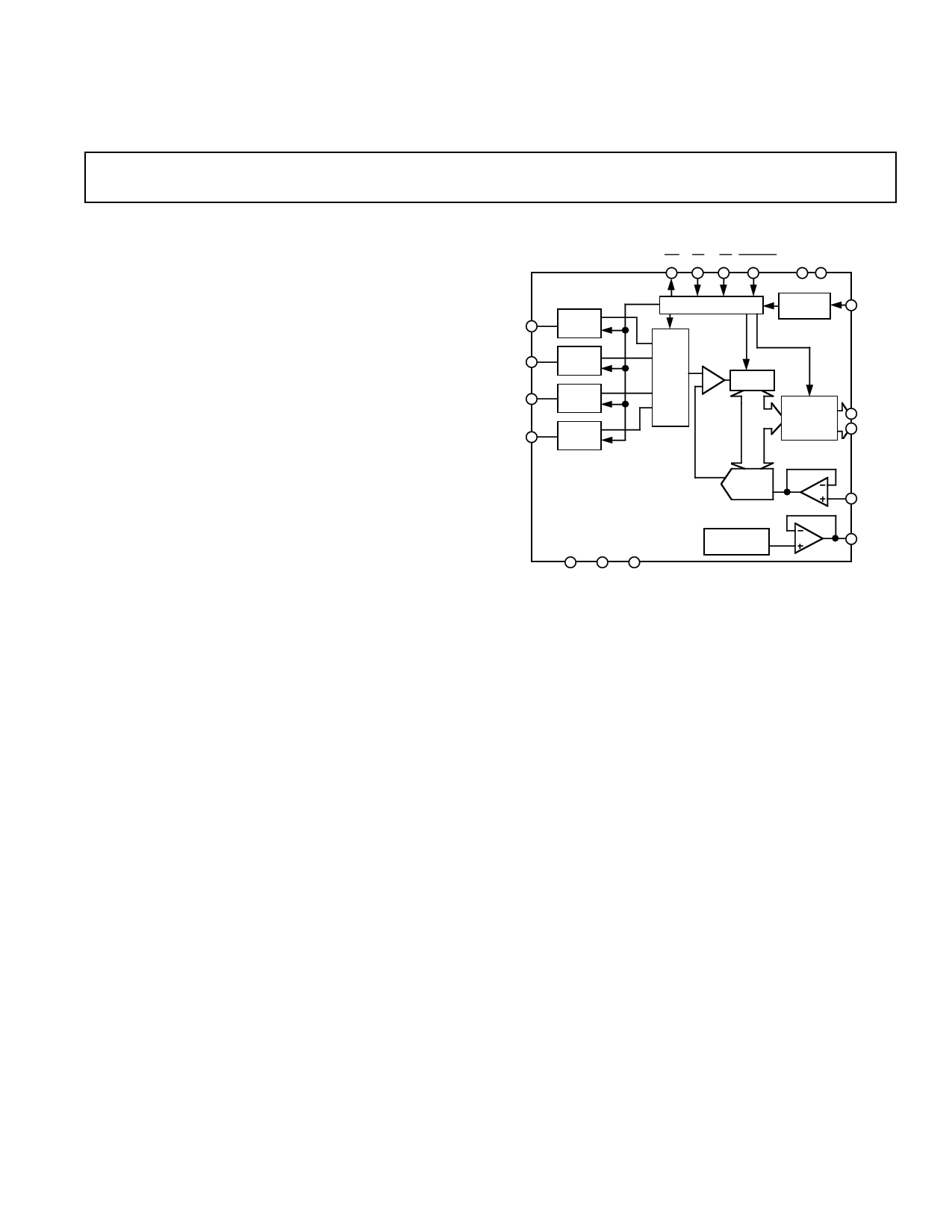
FUNCTIONAL BLOCK DIAGRAM
INT CS RD CONVST VDD VDD
VIN1
TRACK/
HOLD 1
CONTROL LOGIC
INTERNAL
CLOCK
CLK
VIN2
TRACK/
HOLD 2
VIN3
TRACK/
HOLD 3
VIN4
TRACK/
HOLD 4
MUX
COMP
SAR
DATA
REGISTERS
DB0
DB11
REFERENCE
BUFFER
AD7874
12-BIT
DAC
REF IN
3V
REFERENCE
REF OUT
AGND DGND VSS
PRODUCT HIGHLIGHTS
1. Simultaneous Sampling of Four Input Channels.
Four input channels, each with its own track/hold amplifier,
allow simultaneous sampling of input signals. Track/hold ac-
quisition time is 2 µs, and the conversion time per channel is
8 µs, allowing 29 kHz sample rate for all four channels.
2. Tight Aperture Delay Matching.
The aperture delay for each channel is small and the aperture
delay matching between the four channels is less than 4 ns.
Additionally, the aperture delay specification has upper and
lower limits allowing multiple AD7874s to sample more than
four channels.
3. Fast Microprocessor Interface.
The high speed digital interface of the AD7874 allows direct
connection to all modern 16-bit microprocessors and digital
signal processors.
REV. C
Information furnished by Analog Devices is believed to be accurate and
reliable. However, no responsibility is assumed by Analog Devices for its
use, nor for any infringements of patents or other rights of third parties
which may result from its use. No license is granted by implication or
otherwise under any patent or patent rights of Analog Devices.
One Technology Way, P.O. Box 9106, Norwood, MA 02062-9106, U.S.A.
Tel: 617/329-4700
Fax: 617/326-8703
1 page 
AD7874
PIN FUNCTION DESCRIPTION
Pin Mnemonic
1 VIN1
2 VIN2
3 VDD
4 INT
5 CONVST
6 RD
7
8
9
10
11–13
14
15–21
22
23
24
CS
CLK
VDD
DB11
DB10–DB8
DGND
DB7–DB1
DB0
AGND
REF IN
25 REF OUT
26 VSS
27 VIN3
28 VIN4
Description
Analog Input Channel 1. This is the first of the four input channels to be converted in a con-
version cycle. Analog input voltage range is ± 10 V.
Analog Input Channel 2. Analog input voltage range is ± 10 V.
Positive supply voltage, +5 V ± 5%. This pin should be decoupled to AGND.
Interrupt. Active low logic output indicating converter status. See Figure 7.
Convert Start. Logic Input. A low to high transition on this input puts the track/hold into its
hold mode and starts conversion. The four channels are converted sequentially, Channel 1 to
Channel 4. The CONVST input is asynchronous to CLK and independent of CS and RD.
Read. Active low logic input. This input is used in conjunction with CS low to enable the
data outputs. Four successive reads after a conversion will read the data from the four chan-
nels in the sequence, Channel 1, 2, 3, 4.
Chip Select. Active low logic input. The device is selected when this input is active.
Clock Input. An external TTL-compatible clock may be applied to this input pin. Alterna-
tively, tying this pin to VSS enables the internal laser trimmed clock oscillator.
Positive Supply Voltage, +5 V ± 5%. Same as Pin 3; both pins must be tied together at the
package. This pin should be decoupled to DGND.
Data Bit 11 (MSB). Three-state TTL output. Output coding is 2s complement.
Data Bit 10 to Data Bit 8. Three-state TTL outputs.
Digital Ground. Ground reference for digital circuitry.
Data Bit 7 to Data Bit 1. Three-state TTL outputs.
Data Bit 0 (LSB). Three-state TTL output.
Analog Ground. Ground reference for track/hold, reference and DAC.
Voltage Reference Input. The reference voltage for the part is applied to this pin. It is inter-
nally buffered, requiring an input current of only ± 1 µA. The nominal reference voltage for
correct operation of the AD7874 is 3 V.
Voltage Reference Output. The internal 3 V analog reference is provided at this pin. To oper-
ate the AD7874 with internal reference, REF OUT is connected to REF IN. The external
load capability of the reference is 500 µA.
Negative Supply Voltage, –5 V ± 5%.
Analog Input Channel 3. Analog input voltage range is ± 10 V.
Analog Input Channel 4. Analog input voltage range is ± 10 V.
Model1
ORDERING GUIDE
Relative
Temperature
Range
SNR
(dBs)
Accuracy
(LSB)
Package
Option2
AD7874AN
AD7874BN
AD7874AR
AD7874BR
AD7874AQ
AD7874BQ
AD7874SQ3
AD7874SE3
–40°C to +85°C
–40°C to +85°C
–40°C to +85°C
–40°C to +85°C
–40°C to +85°C
–40°C to +85°C
–55°C to +125°C
–55°C to +125°C
70 min
72 min
70 min
72 min
70 min
72 min
70 min
70 min
± 1 max
± 1/2 max
± 1 max
± 1/2 max
± 1 max
± 1/2 max
± 1 max
± 1 max
N-28
N-28
R-28
R-28
Q-28
Q-28
Q-28
E-28A
NOTES
1To order MIL-STD-883, Class B processed parts, add /883B to part number. Contact
1our local sales office for military data sheet and availability.
2E = Leaded Ceramic Chip Carrier; N = Plastic DIP; Q = Cerdip; R = SOIC.
3Available to /883B processing only.
REV. C
–5–
5 Page 
AD7874
Some applications may require that the conversion is initiated
by the microprocessor rather than an external timer. One option
is to decode the AD7874 CONVST from the address bus so
that a write operation starts a conversion. Data is read at the
end of the conversion sequence as before. Figure 16 shows an
example of initiating conversion using this method. Note that
for all interfaces, a read operation should not be attempted dur-
ing conversion.
AD7874–MC68000 Interface
An interface between the AD7874 and the MC68000 is shown
in Figure 15. As before, conversion is initiated using an external
timer. The AD7874 INT line can be used to interrupt the pro-
cessor or, alternatively, software delays can ensure that conver-
sion has been completed before a read to the AD7874 is
attempted. Because of the nature of its interrupts, the 68000
requires additional logic (not shown in Figure 15) to allow it to
be interrupted correctly. For further information on 68000 in-
terrupts, consult the 68000 users manual.
The MC68000 AS and R/W outputs are used to generate a
separate RD input signal for the AD7874. CS is used to drive
the 68000 DTACK input to allow the processor to execute a
normal read operation to the AD7874. The conversion results
are read using the following 68000 instruction:
MOVE.W ADC,D0
where D0 is the 68000 D0 register and
ADC is the AD7874 address.
A15
A0
MC68000
DTACK
ADDRESS BUS
ADDR
DECODE
EN
TIMER
CONVST
CS
AD7874*
AD7874–8086 Interface
Figure 16 shows an interface between the AD7874 and the 8086
microprocessor. Unlike the previous interface examples, the
microprocessor initiates conversion. This is achieved by gating
the 8086 WR signal with a decoded address output (different to
the AD7874 CS address). The AD7874 INT line is used to in-
terrupt the microprocessor when the conversion sequence is
completed. Data is read from the AD7874 using the following
instruction:
MOV AX,ADC
where AX is the 8086 accumulator and
ADC is the AD7874 address.
ADDRESS BUS
8086
ADDR
DECODE
CS
ALE
LATCH
WR
RD
AD7874*
CONVST
RD
DB11
DB0
AD15
AD0
ADDRESS/DATA BUS
*ADDITIONAL PINS OMITTED FOR CLARITY
Figure 16. AD7874–8086 Interface
AS
RD
R/W
DB11
DB0
D15
D0
DATA BUS
*ADDITIONAL PINS OMITTED FOR CLARITY
Figure 15. AD7874–MC68000 Interface
REV. C
–11–
11 Page | ||
| Páginas | Total 16 Páginas | |
| PDF Descargar | [ Datasheet AD7874.PDF ] | |
Hoja de datos destacado
| Número de pieza | Descripción | Fabricantes |
| AD7870 | LC2MOS Complete/ 12-Bit/ 100 kHz/ Sampling ADCs | Analog Devices |
| AD7870A | LC2MOS Complete/ 12-Bit/ 100 kHz / Sampling ADC | Analog Devices |
| AD7871 | LC2MOS Complete 14-Bit/ Sampling ADCs | Analog Devices |
| AD7872 | LC2MOS Complete 14-Bit/ Sampling ADCs | Analog Devices |
| Número de pieza | Descripción | Fabricantes |
| SLA6805M | High Voltage 3 phase Motor Driver IC. |
Sanken |
| SDC1742 | 12- and 14-Bit Hybrid Synchro / Resolver-to-Digital Converters. |
Analog Devices |
|
DataSheet.es es una pagina web que funciona como un repositorio de manuales o hoja de datos de muchos de los productos más populares, |
| DataSheet.es | 2020 | Privacy Policy | Contacto | Buscar |