|
|
|
PDF AD7819 Data sheet ( Hoja de datos )
| Número de pieza | AD7819 | |
| Descripción | +2.7 V to +5.5 V/ 200 kSPS 8-Bit Sampling ADC | |
| Fabricantes | Analog Devices | |
| Logotipo | ||
Hay una vista previa y un enlace de descarga de AD7819 (archivo pdf) en la parte inferior de esta página. Total 11 Páginas | ||
|
No Preview Available !
a
FEATURES
8-Bit ADC with 4.5 s Conversion Time
On-Chip Track and Hold
Operating Supply Range: +2.7 V to +5.5 V
Specifications at +2.7 V – 3.6 V and 5 V ؎ 10%
8-Bit Parallel Interface
8-Bit Read
Power Performance
Normal Operation
10.5 mW, VDD = 3 V
Automatic Power-Down
57.75 W @ 1 kSPS, VDD = 3 V
Analog Input Range: 0 V to VREF
Reference Input Range: 1.2 V to VDD
+2.7 V to +5.5 V, 200 kSPS
8-Bit Sampling ADC
AD7819
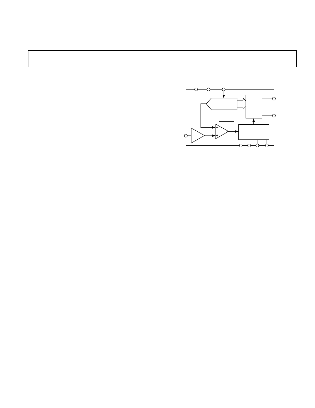
FUNCTIONAL BLOCK DIAGRAM
VDD AGND
VREF
AD7819
CHARGE
REDISTRIBUTION
DAC
CLOCK
OSC
THREE-
STATE
DRIVERS
DB7
DB0
VIN T/H
COMP
CONTROL
LOGIC
BUSY CS RD CONVST
GENERAL DESCRIPTION
The AD7819 is a high speed, microprocessor-compatible, 8-bit
analog-to-digital converter with a maximum throughput of
200 kSPS. The converter operates off a single +2.7 V to +5.5 V
supply and contains a 4.5 µs successive approximation A/D
converter, track/hold circuitry, on-chip clock oscillator and 8-bit
wide parallel interface. The parallel interface is designed to
allow easy interfacing to microprocessors and DSPs. Using only
address decoding logic the AD7819 is easily mapped into the
microprocessor address space.
When used in its power-down mode, the AD7819 automatically
powers down at the end of a conversion and powers up at the
start of a new conversion. This feature significantly reduces the
power consumption of the part at lower throughput rates. The
AD7819 can also operate in a high speed mode where the part is
not powered down between conversions. In this mode of opera-
tion the part is capable of providing 200 kSPS throughput.
The part is available in a small, 16-pin 0.3" wide, plastic dual-
in-line package (DIP); in a 16-pin, 0.15" wide, narrow body
small outline IC (SOIC) and in a 16-pin, narrow body, thin
shrink small outline package (TSSOP).
PRODUCT HIGHLIGHTS
1. Low Power, Single Supply Operation
The AD7819 operates from a single +2.7 V to +5.5 V sup-
ply and typically consumes only 10.5 mW of power. The
power dissipation can be significantly reduced at lower
throughput rates by using the automatic power-down mode.
2. Automatic Power-Down
The automatic power-down mode, whereby the AD7819
goes into power-down mode at the end of a conversion and
powers up before the next conversion, means the AD7819
is ideal for battery powered applications; e.g., 57.75 µW
@ 1 kSPS. (See Power vs. Throughput Rate section.)
3. Parallel Interface
An easy to use 8-bit wide parallel interface allows interfacing
to most popular microprocessors and DSPs with minimal
external circuitry.
4. Dynamic Specifications for DSP Users
In addition to the traditional ADC specifications, the AD7819
is specified for ac parameters, including signal-to-noise ratio
and distortion.
REV. A
Information furnished by Analog Devices is believed to be accurate and
reliable. However, no responsibility is assumed by Analog Devices for its
use, nor for any infringements of patents or other rights of third parties
which may result from its use. No license is granted by implication or
otherwise under any patent or patent rights of Analog Devices.
One Technology Way, P.O. Box 9106, Norwood, MA 02062-9106, U.S.A.
Tel: 781/329-4700 World Wide Web Site: http://www.analog.com
Fax: 781/326-8703
© Analog Devices, Inc., 2000
1 page 
TERMINOLOGY
Signal to (Noise + Distortion) Ratio
This is the measured ratio of signal to (noise + distortion) at the
output of the A/D converter. The signal is the rms amplitude of
the fundamental. Noise is the rms sum of all nonfundamental
signals up to half the sampling frequency (fS/2), excluding dc.
The ratio is dependent upon the number of quantization levels
in the digitization process; the more levels, the smaller the quan-
tization noise. The theoretical signal to (noise + distortion)
ratio for an ideal N-bit converter with a sine wave input is given
by:
Signal to (Noise + Distortion) = (6.02N + 1.76) dB
Thus for an 8-bit converter, this is 50 dB.
Total Harmonic Distortion
Total harmonic distortion (THD) is the ratio of the rms sum of
harmonics to the fundamental. For the AD7819 it is defined as:
THD (dB) = 20 log
V
2
2
+
V
2
3
+
V
2
4
+
V
2
5
+
V
2
6
V1
where V1 is the rms amplitude of the fundamental and V2, V3,
V4, V5 and V6 are the rms amplitudes of the second through the
sixth harmonics.
Peak Harmonic or Spurious Noise
Peak harmonic or spurious noise is defined as the ratio of the
rms value of the next largest component in the ADC output
spectrum (up to fS/2 and excluding dc) to the rms value of the
fundamental. Normally, the value of this specification is deter-
mined by the largest harmonic in the spectrum, but for parts
where the harmonics are buried in the noise floor, it will be a
noise peak.
Intermodulation Distortion
With inputs consisting of sine waves at two frequencies, fa and
fb, any active device with nonlinearities will create distortion
products at sum and difference frequencies of mfa ± nfb where
m, n = 0, 1, 2, 3, etc. Intermodulation terms are those for which
neither m nor n are equal to zero. For example, the second order
terms include (fa + fb) and (fa – fb), while the third order terms
include (2fa + fb), (2fa – fb), (fa + 2fb) and (fa – 2fb).
The AD7819 is tested using the CCIF standard, where two
input frequencies near the top end of the input bandwidth are
used. In this case, the second and third order terms are of differ-
ent significance. The second order terms are usually distanced
in frequency from the original sine waves, while the third order
terms are usually at a frequency close to the input frequencies.
As a result, the second and third order terms are specified sepa-
rately. The calculation of the intermodulation distortion is as
per the THD specification where it is the ratio of the rms sum of
the individual distortion products to the rms amplitude of the
fundamental expressed in dBs.
AD7819
Relative Accuracy
Relative accuracy or endpoint nonlinearity is the maximum
deviation from a straight line passing through the endpoints of
the ADC transfer function.
Differential Nonlinearity
This is the difference between the measured and the ideal
1 LSB change between any two adjacent codes in the ADC.
Offset Error
This is the deviation of the first code transition (0000 . . . 000)
to (0000 . . . 001) from the ideal, i.e., AGND + 1 LSB.
Offset Error Match
This is the difference in Offset Error between any two channels.
Gain Error
This is the deviation of the last code transition (1111 . . . 110)
to (1111 . . . 111) from the ideal, i.e., VREF – 1 LSB, after the
offset error has been adjusted out.
Gain Error Match
This is the difference in Gain Error between any two channels.
Track/Hold Acquisition Time
Track/hold acquisition time is the time required for the output
of the track/hold amplifier to reach its final value, within
± 1/2 LSB, after the end of conversion (the point at which the
track/hold returns to track mode). It also applies to situations
where a change in the selected input channel takes place or
where there is a step input change on the input voltage applied
to the selected VIN input of the AD7819. It means that the user
must wait for the duration of the track/hold acquisition time
after the end of conversion or after a step input change to VIN
before starting another conversion, to ensure that the part
operates to specification.
REV. A
–5–
5 Page 
OUTLINE DIMENSIONS
Dimensions shown in inches and (mm).
16-Lead Plastic DIP
(N-16)
0.840 (21.33)
0.745 (18.93)
16
1
PIN 1
0.210 (5.33)
MAX
0.160 (4.06)
0.115 (2.93)
0.022 (0.558)
0.014 (0.356)
0.100
(2.54)
BSC
9 0.280 (7.11)
8 0.240 (6.10)
0.060 (1.52)
0.015 (0.38)
0.325 (8.25)
0.300 (7.62) 0.195 (4.95)
0.115 (2.93)
0.130
(3.30)
MIN
0.070 (1.77) SEATING
0.045 (1.15) PLANE
0.015 (0.381)
0.008 (0.204)
16-Lead Small Outline Package
(R-16A)
0.3937 (10.00)
0.3859 (9.80)
0.1574 (4.00) 16
0.1497 (3.80) 1
9
0.2550 (6.20)
8 0.2284 (5.80)
0.0098 (0.25)
0.0040 (0.10)
PIN 1
0.0688 (1.75)
0.0532 (1.35)
0.0196 (0.50) ؋ 45°
0.0099 (0.25)
SEATING
PLANE
0.0500
(1.27)
BSC
0.0192 (0.49)
0.0138 (0.35)
8°
0°
0.0099 (0.25)
0.0500 (1.27)
0.0075 (0.19) 0.0160 (0.41)
16-Lead Thin Shrink Small Outline Package
(RU-16)
0.201 (5.10)
0.193 (4.90)
16 9
1
8
0.006 (0.15)
0.002 (0.05)
PIN 1
0.0256 0.0118 (0.30)
SEATING (0.65)
PLANE BSC
0.0075 (0.19)
0.0433
(1.10)
MAX
8°
0.0079 (0.20) 0°
0.0035 (0.090)
0.028 (0.70)
0.020 (0.50)
AD7819
REV. A
–11–
11 Page | ||
| Páginas | Total 11 Páginas | |
| PDF Descargar | [ Datasheet AD7819.PDF ] | |
Hoja de datos destacado
| Número de pieza | Descripción | Fabricantes |
| AD781 | Complete 700 ns Sample-and-Hold Amplifier | Analog Devices |
| AD7810 | 10-Bit ADC | Analog Devices |
| AD7811 | 10-Bit 4-/8-Channel Sampling ADCs | Analog Devices |
| AD7812 | 10-Bit 4-/8-Channel Sampling ADCs | Analog Devices |
| Número de pieza | Descripción | Fabricantes |
| SLA6805M | High Voltage 3 phase Motor Driver IC. |
Sanken |
| SDC1742 | 12- and 14-Bit Hybrid Synchro / Resolver-to-Digital Converters. |
Analog Devices |
|
DataSheet.es es una pagina web que funciona como un repositorio de manuales o hoja de datos de muchos de los productos más populares, |
| DataSheet.es | 2020 | Privacy Policy | Contacto | Buscar |