|
|
|
PDF AD7655 Data sheet ( Hoja de datos )
| Número de pieza | AD7655 | |
| Descripción | PulSAR ADC | |
| Fabricantes | Analog Devices | |
| Logotipo | ||
Hay una vista previa y un enlace de descarga de AD7655 (archivo pdf) en la parte inferior de esta página. Total 26 Páginas | ||
|
No Preview Available !
Data Sheet
FEATURES
4-channel, 16-bit resolution ADC
2 track-and-hold amplifiers
Throughput
500 kSPS (normal mode)
444 kSPS (impulse mode)
Analog input voltage range: 0 V to 5 V
No pipeline delay
Parallel and serial 5 V/3 V interface
SPI®/QSPI™/MICROWIRE™/DSP compatible
Single 5 V supply operation
Power dissipation
120 mW typical
2.6 mW at 10 kSPS
Package
48-lead quad flat package (LQFP)
48-lead frame chip scale package (LFCSP)
Pin-to-pin compatible with the AD7654
Low cost
APPLICATIONS
AC motor control
3-phase power control
4-channel data acquisition
Uninterrupted power supplies
Communications
GENERAL DESCRIPTION
The AD7655 is a low cost, simultaneous sampling, dual-channel,
16-bit, charge redistribution SAR, analog-to-digital converter
that operates from a single 5 V power supply. It contains two
low noise, wide bandwidth, track-and-hold amplifiers that allow
simultaneous sampling, a high speed 16-bit sampling ADC, an
internal conversion clock, error correction circuits, and both
serial and parallel system interface ports. Each track-and-hold
has a multiplexer in front to provide a 4-channel input ADC.
The A0 multiplexer control input allows the choice of
simultaneously sampling input pairs INA1/INB1 (A0 = low) or
INA2/INB2 (A0 = high). The part features a very high sampling
rate mode (normal) and, for low power applications, a reduced
power mode (impulse) where the power is scaled with the
throughput. Operation is specified from −40°C to +85°C.
Low Cost, 4-Channel,
16-Bit, 500 kSPS PulSAR ADC
AD7655
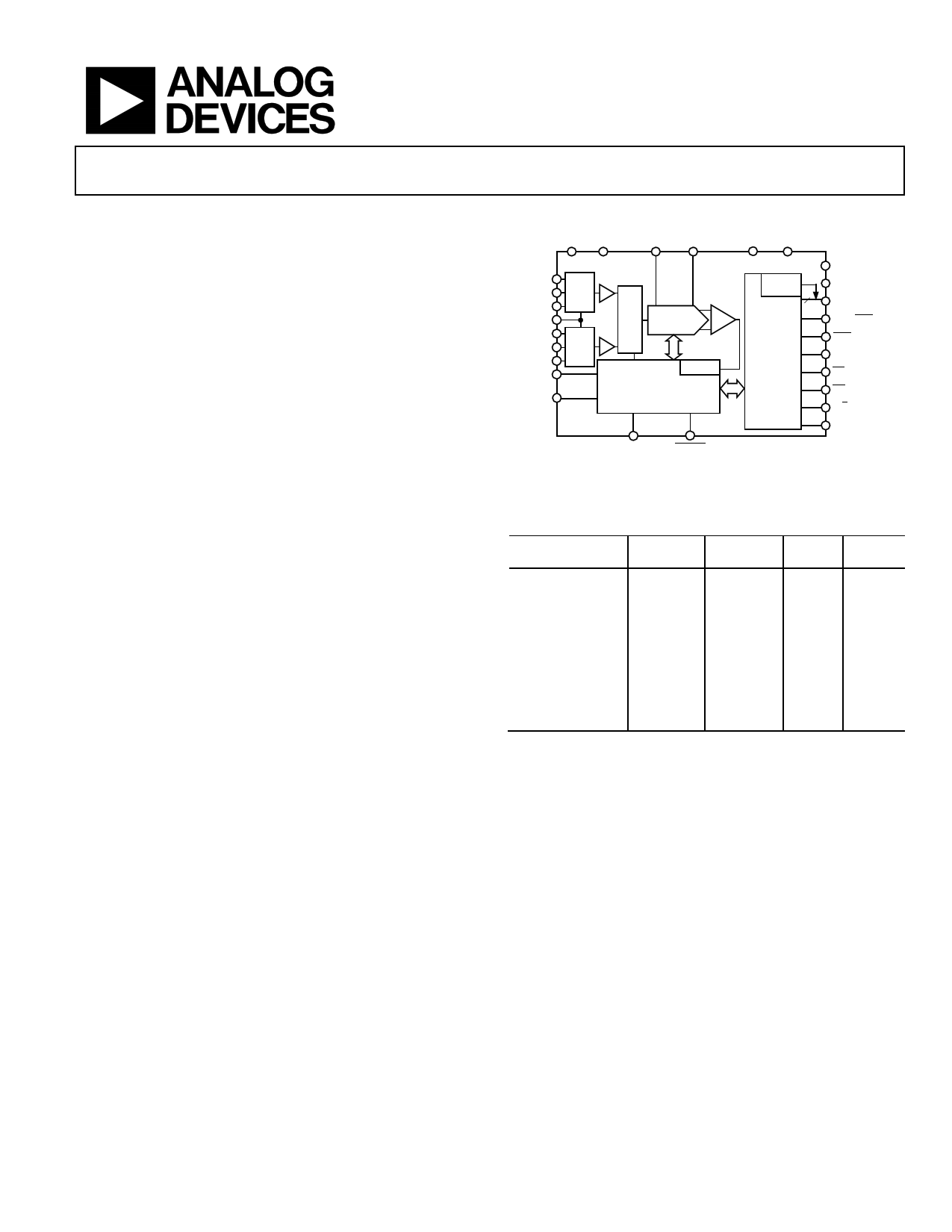
FUNCTIONAL BLOCK DIAGRAM
AVDD AGND REFGND REFx
DVDD DGND
INA1
INAN
INA2
A0
INB1
INBN
INB2
PD
RESET
TRACK/HOLD
×2
MUX
MUX SWITCHED
CAP DAC
MUX
CLOCK
CONTROL LOGIC AND
CALIBRATION CIRCUITRY
AD7655
SERIAL
PORT 16
PARALLEL
INTERFACE
OVDD
OGND
D[15:0]
SER/PAR
EOC
BUSY
CS
RD
A/B
BYTESWAP
IMPULSE
CNVST
Figure 1.
Table 1. PulSAR® Selection
Type/kSPS
Pseudo Differential
100 to 250
AD7660/
AD7661
True Bipolar
True Differential
18 Bit
Multichannel/
Simultaneous
AD7663
AD7675
AD7678
500 to 570
AD7650/
AD7652
AD7664/
AD7666
AD7665
AD7676
AD7679
AD7654/
AD7655
800 to
1000
AD7653
AD7667
AD7671
AD7677
AD7674
>1000
AD7621
AD7623
AD7641
PRODUCT HIGHLIGHTS
1. Multichannel ADC.
The AD7655 features 4-channel inputs with two
sample-and-hold circuits that allow simultaneous sampling.
2. Fast Throughput.
The AD7655 is a 500 kSPS, charge redistribution, 16-bit
SAR ADC with internal error correction circuitry.
3. Single-Supply Operation.
The AD7655 operates from a single 5 V supply. In impulse
mode, its power dissipation decreases with throughput.
4. Serial or Parallel Interface.
Versatile parallel or 2-wire serial interface arrangements
are compatible with both 3 V and 5 V logic.
Rev. E
Document Feedback
Information furnished by Analog Devices is believed to be accurate and reliable. However, no
responsibility is assumed by Analog Devices for its use, nor for any infringements of patents or other
rights of third parties that may result from its use. Specifications subject to change without notice. No
license is granted by implication or otherwise under any patent or patent rights of Analog Devices.
Trademarks and registered trademarks are the property oftheir respective owners.
One Technology Way, P.O. Box 9106, Norwood, MA 02062-9106, U.S.A.
Tel: 78 1.32 9.47 00 ©2002–2016 Analog Devices, Inc. All rights reserved.
Technica l Support
www.analog.com
1 page 
Data Sheet
AD7655
TIMING SPECIFICATIONS
AVDD = DVDD = 5 V, OVDD = 2.7 V to 5.25 V; VREF = 2.5 V; all specifications TMIN to TMAX, unless otherwise noted.
Table 3.
Parameter
CONVERSION AND RESET (See Figure 22 and Figure 23)
Convert Pulse Width
Time Between Conversions
(Normal Mode/Impulse Mode)
CNVST Low to BUSY High Delay
BUSY High All Modes Except in Master Serial Read After Convert Mode
(Normal Mode/Impulse Mode)
Aperture Delay
End of Conversions to BUSY Low Delay
Conversion Time
(Normal Mode/Impulse Mode)
Acquisition Time
RESET Pulse Width
CNVST Low to EOC High Delay
EOC High for Channel A Conversion
(Normal Mode/Impulse Mode)
EOC Low after Channel A Conversion
EOC High for Channel B Conversion
Channel Selection Setup Time
Channel Selection Hold Time
PARALLEL INTERFACE MODES (See Figure 24 to Figure 28)
CNVST Low to DATA Valid Delay
DATA Valid to BUSY Low Delay
Bus Access Request to DATA Valid
Bus Relinquish Time
A/B Low to Data Valid Delay
MASTER SERIAL INTERFACE MODES (See Figure 29 and Figure 30)
CS Low to SYNC Valid Delay
CS Low to Internal SCLK Valid Delay1
CS Low to SDOUT Delay
CNVST Low to SYNC Delay, Read During Convert
(Normal Mode/Impulse Mode)
SYNC Asserted to SCLK First Edge Delay
Internal SCK Period2
Internal SCLK High2
Internal SCLK Low2
SDOUT Valid Setup Time2
SDOUT Valid Hold Time2
SCLK Last Edge to SYNC Delay2
CS High to SYNC HI-Z
CS High to Internal SCLK HI-Z
CS High to SDOUT HI-Z
BUSY High in Master Serial Read after Convert2
CNVST Low to SYNC Asserted Delay
(Normal Mode/Impulse Mode)
SYNC Deasserted to BUSY Low Delay
Symbol Min
Typ
Max
t1 5
t2 2/2.25
t3
32
t4
t5 2
t6 10
t7
t8 250
t9 10
t10
1.75/2
1.75/2
30
t11
t12 45
t13
t14 250
t15
1/1.25
0.75
30
t16
t17 14
t18
t19 5
t20
1.75/2
40
15
40
t21 10
t22 10
t23 10
t24 250/500
t25 3
t26 23
t27 12
40
t28 7
t29 4
t30 2
t31 1
t32 10
t33 10
t34 10
t35 See Table 4
t36 0.75/1
t37 25
Unit
ns
µs
ns
µs
ns
ns
µs
ns
ns
ns
µs
ns
µs
ns
ns
µs
ns
ns
ns
ns
ns
ns
ns
ns
ns
ns
ns
ns
ns
ns
ns
ns
ns
ns
µs
ns
Rev. E | Page 5 of 26
5 Page 
Data Sheet
TERMINOLOGY
Integral Nonlinearity Error (INL)
Linearity error refers to the deviation of each individual code
from a line drawn from negative full scale through positive full
scale. The point used as negative full scale occurs ½ LSB before
the first code transition. Positive full scale is defined as a level
1½ LSBs beyond the last code transition. The deviation is
measured from the middle of each code to the true straight line.
Differential Nonlinearity Error (DNL)
In an ideal ADC, code transitions are 1 LSB apart. Differential
nonlinearity is the maximum deviation from this ideal value,
and is often specified in terms of resolution for which no
missing codes are guaranteed.
Full-Scale Error
The last transition (from 111. . .10 to 111. . .11) should occur for
an analog voltage 1½ LSBs below the nominal full scale
(4.999886 V for the 0 V to 5 V range). The full-scale error is the
deviation of the actual level of the last transition from the ideal
level.
Unipolar Zero Error
The first transition should occur at a level ½ LSB above analog
ground (76.29 µV for the 0 V to 5 V range). The unipolar zero
error is the deviation of the actual transition from that point.
Signal-to-Noise Ratio (SNR)
SNR is the ratio of the rms value of the actual input signal to the
rms sum of all other spectral components below the Nyquist
frequency, excluding harmonics and dc. The value for SNR is
expressed in decibels.
AD7655
Total Harmonic Distortion (THD)
THD is the ratio of the rms sum of the first five harmonic
components to the rms value of a full-scale input signal and is
expressed in decibels.
Signal-to-Noise and Distortion Ratio (SINAD)
SINAD is the ratio of the rms value of the actual input signal to
the rms sum of all other spectral components below the Nyquist
frequency, including harmonics but excluding dc. The value for
SINAD is expressed in decibels.
Spurious-Free Dynamic Range (SFDR)
The difference, in decibels, between the rms amplitude of the
input signal and the peak spurious signal.
Effective Number of Bits (ENOB)
ENOB is a measurement of the resolution with a sine wave
input. It is related to SINAD and expressed in bits by
ENOB = (SINADdB − 1.76)/6.02
Aperture Delay
Aperture delay is a measure of acquisition performance and is
measured from the falling edge of the CNVST input to when
the input signals are held for a conversion.
Transient Response
The time required for the AD7655 to achieve its rated accuracy
after a full-scale step function is applied to its input.
Rev. E | Page 11 of 26
11 Page | ||
| Páginas | Total 26 Páginas | |
| PDF Descargar | [ Datasheet AD7655.PDF ] | |
Hoja de datos destacado
| Número de pieza | Descripción | Fabricantes |
| AD7650 | Low Cost CMOS ADC | Analog Devices |
| AD7651 | Unipolar ADC | Analog Devices |
| AD7652 | Unipolar ADC | Analog Devices |
| AD7653 | 16-Bit 1 MSPS SAR Unipolar ADC | Analog Devices |
| Número de pieza | Descripción | Fabricantes |
| SLA6805M | High Voltage 3 phase Motor Driver IC. |
Sanken |
| SDC1742 | 12- and 14-Bit Hybrid Synchro / Resolver-to-Digital Converters. |
Analog Devices |
|
DataSheet.es es una pagina web que funciona como un repositorio de manuales o hoja de datos de muchos de los productos más populares, |
| DataSheet.es | 2020 | Privacy Policy | Contacto | Buscar |