|
|
|
PDF AD9764 Data sheet ( Hoja de datos )
| Número de pieza | AD9764 | |
| Descripción | TxDAC D/A Converter | |
| Fabricantes | Analog Devices | |
| Logotipo | ||
Hay una vista previa y un enlace de descarga de AD9764 (archivo pdf) en la parte inferior de esta página. Total 23 Páginas | ||
|
No Preview Available !
a
14-Bit, 125 MSPS
TxDAC® D/A Converter
AD9764
FEATURES
Member of Pin-Compatible TxDAC Product Family
125 MSPS Update Rate
14-Bit Resolution
Excellent SFDR and IMD
Differential Current Outputs: 2 mA to 20 mA
Power Dissipation: 190 mW @ 5 V to 45 mW @ 3 V
Power-Down Mode: 25 mW @ 5 V
On-Chip 1.20 V Reference
Single +5 V or +3 V Supply Operation
Packages: 28-Lead SOIC and TSSOP
Edge-Triggered Latches
APPLICATIONS
Communication Transmit Channel:
Basestations
ADSL/HFC Modems
Instrumentation
PRODUCT DESCRIPTION
The AD9764 is the 14-bit resolution member of the TxDAC
series of high performance, low power CMOS digital-to-analog
converters (DACs). The TxDAC family, which consists of pin
compatible 8-, 10-, 12-, and 14-bit DACs, is specifically opti-
mized for the transmit signal path of communication systems.
All of the devices share the same interface options, small outline
package and pinout, providing an upward or downward compo-
nent selection path based on performance, resolution and cost.
The AD9764 offers exceptional ac and dc performance while
supporting update rates up to 125 MSPS.
The AD9764’s flexible single-supply operating range of 2.7 V to
5.5 V and low power dissipation are well suited for portable and
low power applications. Its power dissipation can be further
reduced to a mere 45 mW with a slight degradation in performance
by lowering the full-scale current output. Also, a power-down
mode reduces the standby power dissipation to approximately
25 mW.
The AD9764 is manufactured on an advanced CMOS process.
A segmented current source architecture is combined with a
proprietary switching technique to reduce spurious components
and enhance dynamic performance. Edge-triggered input
latches and a 1.2 V temperature compensated bandgap refer-
ence have been integrated to provide a complete monolithic
DAC solution. Flexible supply options support +3 V and +5 V
CMOS logic families.
The AD9764 is a current-output DAC with a nominal full-scale
output current of 20 mA and > 100 kΩ output impedance.
TxDAC is a registered trademark of Analog Devices, Inc.
REV. C
Information furnished by Analog Devices is believed to be accurate and
reliable. However, no responsibility is assumed by Analog Devices for its
use, nor for any infringements of patents or other rights of third parties
which may result from its use. No license is granted by implication or
otherwise under any patent or patent rights of Analog Devices.
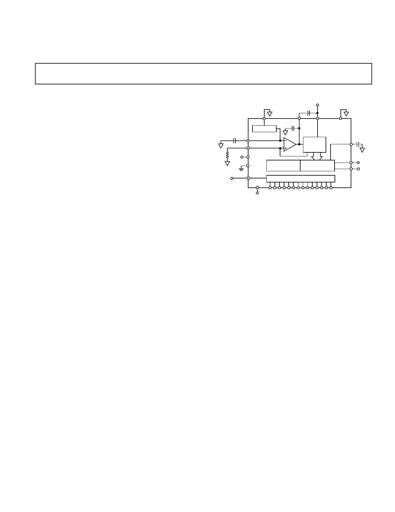
FUNCTIONAL BLOCK DIAGRAM
+5V
0.1F
0.1F
RSET
+5V
CLOCK
REFLO
+1.20V REF
REFIO
FS ADJ
COMP1 AVDD ACOM
50pF
AD9764
CURRENT
SOURCE
ARRAY
0.1F
COMP2
DVDD
DCOM
SEGMENTED
SWITCHES
LSB
SWITCHES
IOUTA
IOUTB
CLOCK
SLEEP
LATCHES
DIGITAL DATA INPUTS (DB13–DB0)
Differential current outputs are provided to support single-
ended or differential applications. Matching between the two
current outputs ensures enhanced dynamic performance in a
differential output configuration. The current outputs may be
tied directly to an output resistor to provide two complemen-
tary, single-ended voltage outputs or fed directly into a trans-
former. The output voltage compliance range is 1.25 V.
The on-chip reference and control amplifier are configured for
maximum accuracy and flexibility. The AD9764 can be driven
by the on-chip reference or by a variety of external reference
voltages. The internal control amplifier, which provides a wide
(>10:1) adjustment span, allows the AD9764 full-scale current
to be adjusted over a 2 mA to 20 mA range while maintaining
excellent dynamic performance. Thus, the AD9764 may operate
at reduced power levels or be adjusted over a 20 dB range to
provide additional gain ranging capabilities.
The AD9764 is available in 28-lead SOIC and TSSOP packages.
It is specified for operation over the industrial temperature range.
PRODUCT HIGHLIGHTS
1. The AD9764 is a member of the TxDAC product family that
provides an upward or downward component selection path
based on resolution (8 to 14 bits), performance and cost.
2. Manufactured on a CMOS process, the AD9764 uses a pro-
prietary switching technique that enhances dynamic perfor-
mance beyond that previously attainable by higher power/cost
bipolar or BiCMOS devices.
3. On-chip, edge-triggered input CMOS latches readily interface
to +3 V and +5 V CMOS logic families. The AD9764 can
support update rates up to 125 MSPS.
4. A flexible single-supply operating range of 2.7 V to 5.5 V, and
a wide full-scale current adjustment span of 2 mA to 20 mA,
allows the AD9764 to operate at reduced power levels.
5. The current output(s) of the AD9764 can be easily config-
ured for various single-ended or differential circuit topologies.
One Technology Way, P.O. Box 9106, Norwood, MA 02062-9106, U.S.A.
Tel:781/329-4700 World Wide Web Site: http://www.analog.com
Fax:781/326-8703
© Analog Devices, Inc., 1999-2016
1 page 
AD9764
DIGITAL SPECIFICATIONS
Parameter
DIGITAL INPUTS
Logic “1” Voltage @ DVDD = +5 V
Logic “1” Voltage @ DVDD = +3 V
Logic “0” Voltage @ DVDD = +5 V
Logic “0” Voltage @ DVDD = +3 V
Logic “1” Current
Logic “0” Current
Input Capacitance
Input Setup Time (tS)
Input Hold Time (tH)
Latch Pulsewidth (tLPW)
Specifications subject to change without notice.
DB0–DB13
CLOCK
IOUTA
OR
IOUTB
Min Typ
3.5 5
2.1 3
0
0
–10
–10
5
2.0
1.5
3.5
tS tH
tLPW
tPD
tST
0.1%
0.1%
Figure 1. Timing Diagram
Max
1.3
0.9
+10
+10
Units
V
V
V
V
µA
µA
pF
ns
ns
ns
ABSOLUTE MAXIMUM RATINGS*
Parameter
With
Respect to Min
Max
Units
ORDERING GUIDE
AVDD
ACOM
–0.3 +6.5
V
DVDD
DCOM
–0.3 +6.5
V
ACOM
DCOM
–0.3 +0.3
V
AVDD
DVDD
–6.5 +6.5
V
CLOCK, SLEEP
DCOM
–0.3 DVDD + 0.3 V
Digital Inputs
DCOM
–0.3 DVDD + 0.3 V
IOUTA, IOUTB
COMP1, COMP2
ACOM
ACOM
–1.0 AVDD + 0.3 V
–0.3 AVDD + 0.3 V
REFIO, FSADJ
ACOM
–0.3 AVDD + 0.3 V
REFLO
ACOM
–0.3 +0.3
V
Junction Temperature
Storage Temperature
Lead Temperature
(10 sec)
+150
–65 +150
+300
°C
°C 1 RW = Small Outline IC, RU = TSSOP.
°C 2 Z = RoHS Compliant Part.
*Stresses above those listed under Absolute Maximum Ratings may cause perma-
nent damage to the device. This is a stress rating only; functional operation of the
device at these or any other conditions above those indicated in the operational
sections of this specification is not implied. Exposure to absolute maximum ratings
for extended periods may affect device reliability.
THERMAL CHARACTERISTICS
Thermal Resistance
28-Lead 300 mil SOIC
θJA = 71.4° C/W
θJC = 23° C/W
28-Lead TSSOP
CAUTION
θJA = 97.9° C/W
θJC = 14.0° C/W
ESD (electrostatic discharge) sensitive device. Electrostatic charges as high as 4000 V readily
accumulate on the human body and test equipment and can discharge without detection.
WARNING!
Although the AD9764 features proprietary ESD protection circuitry, permanent damage may
occur on devices subjected to high energy electrostatic discharges. Therefore, proper ESD
precautions are recommended to avoid performance degradation or loss of functionality.
ESD SENSITIVE DEVICE
–4– REV. C
5 Page 
AD9764
REFERENCE OPERATION
The AD9764 contains an internal 1.20 V bandgap reference
that can be easily disabled and overridden by an external
reference. REFIO serves as either an input or output, depending
on whether the internal or external reference is selected. If
REFLO is tied to ACOM, as shown in Figure 22, the internal
reference is activated, and REFIO provides a 1.20 V output. In
this case, the internal reference must be compensated externally
with a ceramic chip capacitor of 0.1 µF or greater from REFIO
to REFLO. Also, REFIO should be buffered with an external
amplifier having an input bias current less than 100 nA if any
additional loading is required.
OPTIONAL
EXTERNAL
REF BUFFER
REFLO
+5V
0.1F
COMP1 AVDD
ADDITIONAL
LOAD
0.1F
2k⍀
+1.2V REF
REFIO
FS ADJ
AD9764
50pF
CURRENT
SOURCE
ARRAY
provides several application benefits. The first benefit relates
directly to the power dissipation of the AD9764, which is pro-
portional to IOUTFS (refer to the Power Dissipation section). The
second benefit relates to the 20 dB adjustment, which is useful
for system gain control purposes.
The small signal bandwidth of the reference control amplifier is
approximately 1.4 MHz and can be reduced by connecting an
external capacitor between COMP1 and AVDD. The output of
the control amplifier, COMP1, is internally compensated via a
50 pF capacitor that limits the control amplifier small-signal
bandwidth and reduces its output impedance. Any additional
external capacitance further limits the bandwidth and acts as a
filter to reduce the noise contribution from the reference ampli-
fier. Figure 24 shows the relationship between the external
capacitor and the small signal –3 dB bandwidth of the refer-
ence amplifier. Since the –3 dB bandwidth corresponds to the
dominant pole, and hence the time constant, the settling time of
the control amplifier to a stepped reference input response can
be approximated.
1000
Figure 22. Internal Reference Configuration
The internal reference can be disabled by connecting REFLO to
AVDD. In this case, an external reference may then be applied
to REFIO as shown in Figure 23. The external reference may
provide either a fixed reference voltage to enhance accuracy and
drift performance or a varying reference voltage for gain control.
Note that the 0.1 µF compensation capacitor is not required
since the internal reference is disabled, and the high input im-
pedance (i.e., 1 MΩ) of REFIO minimizes any loading of the
external reference.
AVDD
0.1F
AVDD
EXTERNAL
REF
VREFIO
REFLO
+1.2V REF
REFIO
FS ADJ
RSET
IREF =
VREFIO/RSET
AD9764
COMP1 AVDD
50pF
CURRENT
SOURCE
ARRAY
REFERENCE
CONTROL
AMPLIFIER
Figure 23. External Reference Configuration
REFERENCE CONTROL AMPLIFIER
The AD9764 also contains an internal control amplifier that is
used to regulate the DAC’s full-scale output current, IOUTFS.
The control amplifier is configured as a V-I converter, as shown
in Figure 23, such that its current output, IREF, is determined by
the ratio of the VREFIO and an external resistor, RSET, as stated
in Equation 4. IREF is copied over to the segmented current
sources with the proper scaling factor to set IOUTFS as stated in
Equation 3.
The control amplifier allows a wide (10:1) adjustment span of
IOUTFS over a 2 mA to 20 mA range by setting IREF between
62.5 µA and 625 µA. The wide adjustment span of IOUTFS
10
0.1
0.1
1 10 100
COMP1 CAPACITOR – nF
1000
Figure 24. External COMP1 Capacitor vs. –3 dB Bandwidth
The optimum distortion performance for any reconstructed
waveform is obtained with a 0.1 µF external capacitor installed.
Thus, if IREF is fixed for an application, a 0.1 µF ceramic chip
capacitor is recommended. Also, since the control amplifier is
optimized for low power operation, multiplying applications
requiring large signal swings should consider using an external
control amplifier to enhance the application’s overall large signal
multiplying bandwidth and/or distortion performance.
There are two methods in which IREF can be varied for a fixed
RSET. The first method is suitable for a single-supply system in
which the internal reference is disabled, and the common-mode
voltage of REFIO is varied over its compliance range of 1.25 V
to 0.10 V. REFIO can be driven by a single-supply amplifier or
DAC, thus allowing IREF to be varied for a fixed RSET. Since the
input impedance of REFIO is approximately 1 MΩ, a simple,
low cost R-2R ladder DAC configured in the voltage mode
topology may be used to control the gain. This circuit is shown
in Figure 25 using the AD7524 and an external 1.2 V reference,
the AD1580.
–10–
REV. C
11 Page | ||
| Páginas | Total 23 Páginas | |
| PDF Descargar | [ Datasheet AD9764.PDF ] | |
Hoja de datos destacado
| Número de pieza | Descripción | Fabricantes |
| AD976 | 16-Bit/ 100 kSPS/200 kSPS BiCMOS A/D Converters | Analog Devices |
| AD9760 | 10-Bit 125 MSPS TxDAC D/A Converter | Analog Devices |
| AD9761 | Dual 10-Bit TxDAC+ | Analog Devices |
| AD9762 | 12-Bit/ 125 MSPS TxDAC D/A Converter | Analog Devices |
| Número de pieza | Descripción | Fabricantes |
| SLA6805M | High Voltage 3 phase Motor Driver IC. |
Sanken |
| SDC1742 | 12- and 14-Bit Hybrid Synchro / Resolver-to-Digital Converters. |
Analog Devices |
|
DataSheet.es es una pagina web que funciona como un repositorio de manuales o hoja de datos de muchos de los productos más populares, |
| DataSheet.es | 2020 | Privacy Policy | Contacto | Buscar |