|
|
|
PDF AD9696 Data sheet ( Hoja de datos )
| Número de pieza | AD9696 | |
| Descripción | Ultrafast TTL Comparators | |
| Fabricantes | Analog Devices | |
| Logotipo | ||
Hay una vista previa y un enlace de descarga de AD9696 (archivo pdf) en la parte inferior de esta página. Total 8 Páginas | ||
|
No Preview Available !
a
Ultrafast
TTL Comparators
AD9696/AD9698
FEATURES
4.5 ns Propagation Delay
200 ps Maximum Propagation Delay Dispersion
Single +5 V or ؎5 V Supply Operation
Complementary Matched TTL Outputs
APPLICATIONS
High Speed Line Receivers
Peak Detectors
Window Comparators
High Speed Triggers
Ultrafast Pulse Width Discriminators
GENERAL DESCRIPTION
The AD9696 and AD9698 are ultrafast TTL-compatible volt-
age comparators able to achieve propagation delays previously
possible only in high performance ECL devices. The AD9696 is
a single comparator providing 4.5 ns propagation delay, 200 ps
maximum delay dispersion and 1.7 ns setup time. The AD9698
is a dual comparator with equally high performance; both de-
vices are ideal for critical timing circuits in such applications as
ATE, communications receivers and test instruments.
Both devices allow the use of either a single +5 V supply or
± 5 V supplies. The choice of supplies determines the common
mode input voltage range available: –2.2 V to +3.7 V for ± 5 V
operation, +1.4 V to +3.7 V for single +5 V supply operation.
The differential input stage features high precision, with offset
voltages that are less than 2 mV and offset currents less than
1 µA. A latch enable input is provided to allow operation in ei-
ther sample-and-hold or track-and-hold applications.
The AD9696 and AD9698 are both available as commercial
temperature range devices operating from ambient temperatures
of 0°C to +70°C, and as extended temperature range devices for
ambient temperatures from –55°C to +125°C. Both versions are
available qualified to MIL-STD-883 class B.
Package options for the AD9696 include a 10-pin TO-100 metal
can, an 8-pin ceramic DIP, an 8-pin plastic DIP, and an 8-lead
small outline plastic package. The AD9698 is available in a
16-pin ceramic DIP, a 16-lead ceramic gullwing, a 16-pin plastic
DIP and a 16-lead small outline plastic package. Military quali-
fied versions of the AD9696 come in the TO-100 can and
ceramic DIP; the dual AD9698 comes in ceramic DIP.
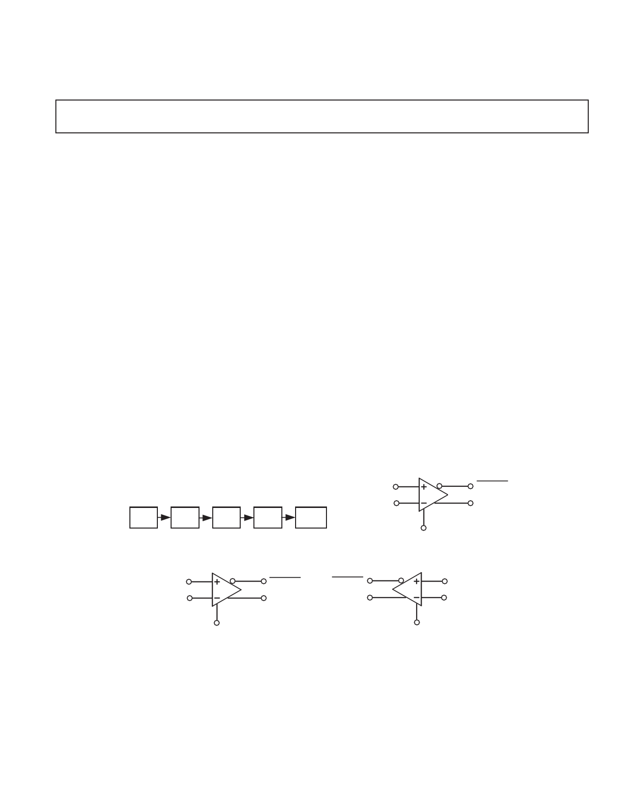
FUNCTIONAL BLOCK DIAGRAM
AD9696/AD9698 Architecture
INPUT
LATCH
GAIN
LEVEL
SHIFT
OUTPUT
NONINVERTING
INPUT
INVERTING
INPUT
AD9698
AD9696
Q OUTPUT
Q OUTPUT
LATCH
ENABLE
NONINVERTING
INPUT
INVERTING
INPUT
#1
Q OUTPUT
Q OUTPUT
Q OUTPUT
Q OUTPUT
NONINVERTING
#2 INPUT
INVERTING
INPUT
LATCH
ENABLE
LATCH
ENABLE
REV. B
Information furnished by Analog Devices is believed to be accurate and
reliable. However, no responsibility is assumed by Analog Devices for its
use, nor for any infringements of patents or other rights of third parties
which may result from its use. No license is granted by implication or
otherwise under any patent or patent rights of Analog Devices.
One Technology Way, P.O. Box 9106, Norwood, MA 02062-9106, U.S.A.
Tel: 617/329-4700
World Wide Web Site: http://www.analog.com
Fax: 617/326-8703
© Analog Devices, Inc., 1997
1 page 
LATCH
ENABLE
LATCH
COMPARE
DIFFERENTIAL
INPUT VOLTAGE
VIN
Q 50%
Q 50%
VOS
tH
VOD
tPD
tPW (E)
tPD (E)
AD9696/AD9698
TWO DIODES
ABOVE GROUND
tS
tS – MINIMUM SETUP TIME (Typically 1.7ns)
t H – MINIMUM HOLD TIME (Typically 1.9ns)
t PD – INPUT TO OUTPUT DELAY
tPD (E) – LATCH ENABLE TO OUTPUT DELAY
tPW (E) – MINIMUM LATCH ENABLE PULSE WIDTH (Typically 2.5ns)
VOS – INPUT OFFSET VOLTAGE
VOD – OVERDRIVE VOLTAGE
AD9696/AD9698 Timing Diagram
DIE LAYOUT AND MECHANICAL INFORMATION
Die Dimensions AD9696 . . . . . . . . . . . . . 59×71×15 (± 2) mils
AD9698 . . . . . . . . . . . . 79×109×15 (± 2) mils
Pad Dimensions . . . . . . . . . . . . . . . . . . . . . . . . . . . . . 4×4 mils
Metalization . . . . . . . . . . . . . . . . . . . . . . . . . . . . . . Aluminum
Backing . . . . . . . . . . . . . . . . . . . . . . . . . . . . . . . . . . . . . None
Substrate Potential . . . . . . . . . . . . . . . . . . . . . . . . . . . . . . . –VS
Passivation . . . . . . . . . . . . . . . . . . . . . . . . . . . . . . . . . . Nitride
THEORY OF OPERATION
Refer to the block diagram of the AD9696/AD9698 compara-
tors. The AD9696 and AD9698 TTL voltage comparator archi-
tecture consists of five basic stages: input, latch, gain, level shift
and output. Each stage is designed to provide optimal perfor-
mance and make it easy to use the comparators.
The input stage operates with either a single +5-volt supply, or
with a +5-volt supply and a –5.2-volt supply. For optimum
power efficiency, the remaining stages operate with only a single
+5-volt supply. The input stage is an input differential pair
without the customary emitter follower buffers. This configura-
tion increases input bias currents but maximizes the input volt-
age range.
A latch stage allows the most recent output state to be retained
as long as the latch input is held high. In this way, the input to
the comparator can be changed without any change in the out-
put state. As soon as the latch enable input is switched to LOW,
the output changes to the new value dictated by the signal ap-
plied to the input stage.
The gain stage assures that even with small values of input volt-
age, there will be sufficient levels applied to the following stages
to cause the output to switch TTL states as required. A level
shift stage between the gain stage and the TTL output stage
guarantees that appropriate voltage levels are applied from the
gain stage to the TTL output stage.
Only the output stage uses TTL logic levels; this minimum use
of TTL circuits maximizes speed and minimizes power con-
sumption. The outputs are clamped with Schottky diodes to as-
sure that the rising and falling edges of the output signal are
closely matched.
The AD9696 and AD9698 represent the state of the art in high
speed TTL voltage comparators. Great care has been taken to
optimize the propagation delay dispersion performance. This as-
sures that the output delays will remain constant despite varying
levels of input overdrive. This characteristic, along with closely
matched rising and falling outputs, provides extremely consis-
tent results at previously unattainable speeds.
REV. B
–5–
5 Page | ||
| Páginas | Total 8 Páginas | |
| PDF Descargar | [ Datasheet AD9696.PDF ] | |
Hoja de datos destacado
| Número de pieza | Descripción | Fabricantes |
| AD9690 | Analog-to-Digital Converter | Analog Devices |
| AD9691 | Dual Analog-to-Digital Converter | Analog Devices |
| AD9694 | Quad Analog-to-Digital Converter | Analog Devices |
| AD9696 | Ultrafast TTL Comparators | Analog Devices |
| Número de pieza | Descripción | Fabricantes |
| SLA6805M | High Voltage 3 phase Motor Driver IC. |
Sanken |
| SDC1742 | 12- and 14-Bit Hybrid Synchro / Resolver-to-Digital Converters. |
Analog Devices |
|
DataSheet.es es una pagina web que funciona como un repositorio de manuales o hoja de datos de muchos de los productos más populares, |
| DataSheet.es | 2020 | Privacy Policy | Contacto | Buscar |