|
|
PDF AD9500 Data sheet ( Hoja de datos )
| Número de pieza | AD9500 | |
| Descripción | Digitally Programmable Delay Generator | |
| Fabricantes | Analog Devices | |
| Logotipo |  |
|
Hay una vista previa y un enlace de descarga de AD9500 (archivo pdf) en la parte inferior de esta página. Total 11 Páginas | ||
|
No Preview Available !
a
Digitally Programmable
Delay Generator
AD9500
FEATURES
10 ps Delay Resolution
2.5 ns to 10 s Full-Scale Range
Fully Differential Inputs
Separate Trigger and Reset Inputs
Low Power Dissipation—310 mW
MIL-STD-883 Compliant Versions Available
APPLICATIONS
ATE
Pulse Deskewing
Arbitrary Waveform Generators
High Stability Timing Source
Multiple Phase Clock Generators
GENERAL DESCRIPTION
The AD9500 is a digitally programmable delay generator, which
provides programmed delays, selected through an 8-bit digital
code, in resolutions as small as 10 ps. The AD9500 is con-
structed in a high performance bipolar process, designed to
provide high speed operation for both digital and analog circuits.
The AD9500 employs differential TRIGGER and RESET
inputs which are designed primarily for ECL signal levels but
function with analog and TTL input levels. An onboard ECL
reference midpoint allows both of the inputs to be driven by
either single ended or differential ECL circuits. The AD9500
output is a complementary ECL stage, which also provides a Q
R
parallel output circuit to facilitate reset timing implementations.
The digital control data is passed to the AD9500 through a
transparent latch controlled by the LATCH ENABLE signal. In
the transparent mode, the internal DAC of the AD9500 will
attempt to follow changes at the inputs. The LATCH ENABLE
is otherwise used to strobe the digital data into the AD9500
latches.
The AD9500 is available as an industrial temperature range
device, –25°C to +85°C, and as an extended temperature range
device, –55°C to +125°C. Both grades are packaged in a 24-lead
cerdip (0.3" package width), as well as 28-leaded and leadless
surface mount packages. The AD9500 is available in versions
compliant with MIL-STD-883. Refer to the Analog Devices
Military Products Databook or current AD9500/883B data
sheet for detailed specifications.
FUNCTIONAL BLOCK DIAGRAM
TRIGGER
TRIGGER
RESET
RESET
DIFFERENTIAL
ANALOG
INPUT
STAGE
+VS
CEXT
CS
ECL COMMON
AD9500
TIMING
CONTROL
CIRCUIT
Q
ECLREF
RS
RSET
–VS
ECL
VOLTAGE
REFERENCE
REFERENCE
CURRENT
INTERNAL DAC
TTL LATCHES
Q
QR
–VS GROUND D0 D1 D2 D3 D4 D5 D6 D7 LATCH OFFSET
(LSB)
(MSB) ENABLE ADJUST
PIN CONFIGURATIONS
D4 1
D5 2
D6 3
D7 (MSB) 4
ECLREF 5
OFFSET ADJUST 6
CS 7
+VS 8
TRIGGER 9
TRIGGER 10
RESET 11
RESET 12
AD9500
TOP VIEW
(Not to Scale)
24 D3
23 D2
22 D1
21 D0 (LSB)
20 LATCH ENABLE
19 GROUND
18 RS
17 –VS
16 ECL COMMON
15 QR
14 Q
13 Q
4 3 2 1 28 27 26
D7 (MSB) 5
ECLREF 6
OFFSET ADJUST 7
NC 8
CS 9
+VS 10
TRIGGER 11
AD9500
TOP VIEW
(Not to Scale)
25 D0 (LSB)
24 LATCH ENABLE
23 GROUND
22 NC
21 RS
20 –VS
19 ECL COMMON
12 13 14 15 16 17 18
REV. D
Information furnished by Analog Devices is believed to be accurate and
reliable. However, no responsibility is assumed by Analog Devices for its
use, nor for any infringements of patents or other rights of third parties
which may result from its use. No license is granted by implication or
otherwise under any patent or patent rights of Analog Devices.
NC = NO CONNECT
One Technology Way, P.O. Box 9106, Norwood, MA 02062-9106, U.S.A.
Tel: 781/329-4700 World Wide Web Site: http://www.analog.com
Fax: 781/326-8703
© Analog Devices, Inc., 1999
1 page 
AD9500
DIE LAYOUT
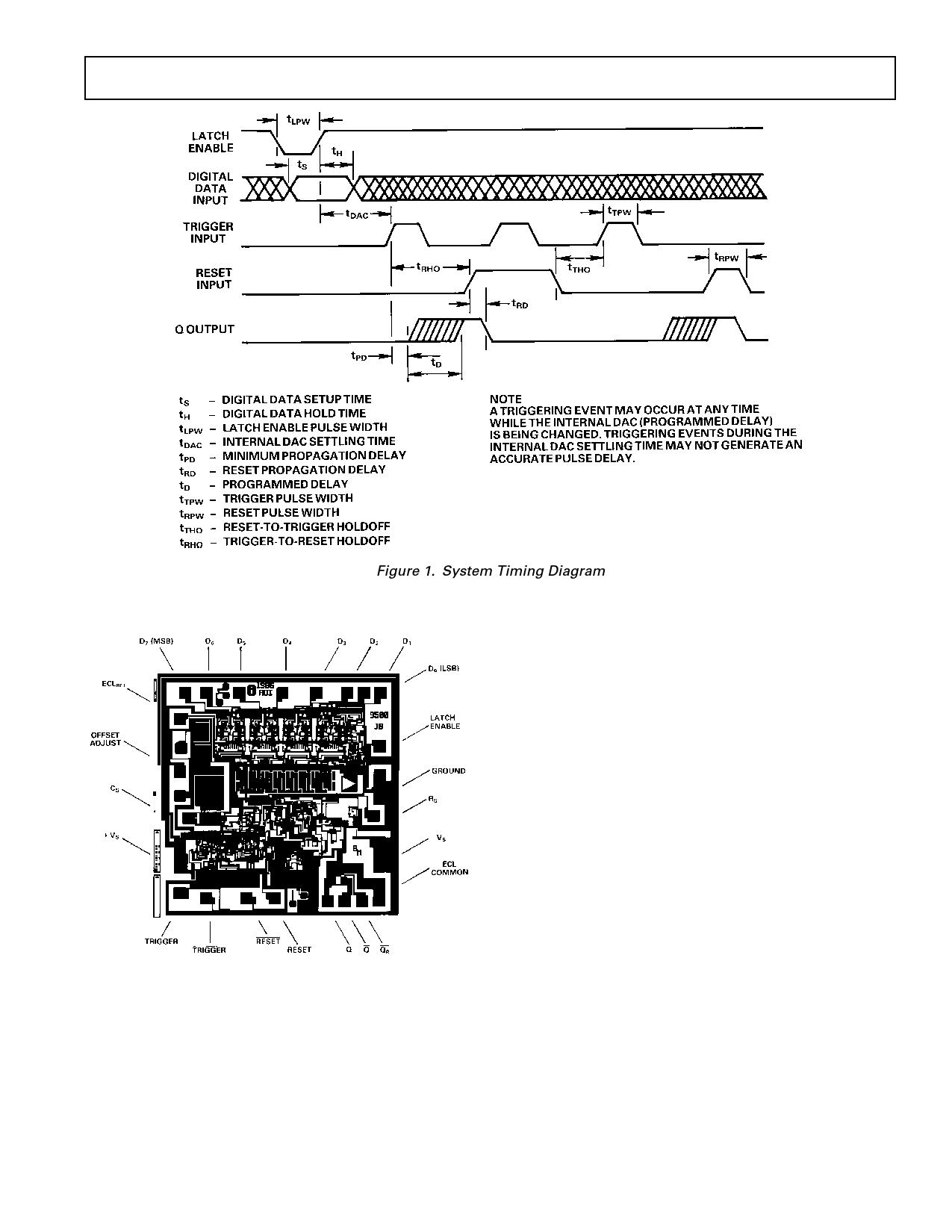
Figure 1. System Timing Diagram
MECHANICAL INFORMATION
Die Dimensions . . . . . . . . . . . . . . . 104 ϫ 103 ϫ 18 (max) mils
Pad Dimensions . . . . . . . . . . . . . . . . . . . . . . . 4 ϫ 4 (min) mils
Metalization . . . . . . . . . . . . . . . . . . . . . . . . . . . . . . . Aluminum
Backing . . . . . . . . . . . . . . . . . . . . . . . . . . . . . . . . . . . . . . None
Substrate Potential . . . . . . . . . . . . . . . . . . . . . . . . . . . . . . .–VS
Passivation . . . . . . . . . . . . . . . . . . . . . . . . . . . . . . . . Oxynitride
Die Attach . . . . . . . . . . . . . . . . . . . . . . . . . . . . . .Gold Eutectic
Bond Wire . . . . . . . . 1.25 mil, Aluminum; Ultrasonic Bonding
or 1 mil, Gold; Gold Ball Bonding
REV. D
–5–
5 Page 
REV. D
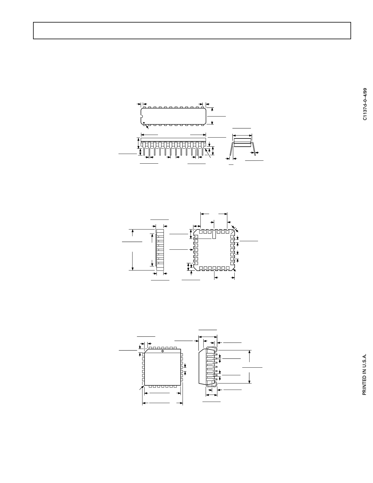
OUTLINE DIMENSIONS
Dimensions shown in inches and (mm).
24-Lead Cerdip
(Q-24)
0.005 (0.13) MIN
0.098 (2.49) MAX
24 13
0.310 (7.87)
1
PIN 1
1.280 (32.51) MAX
0.220 (5.59)
12
0.060 (1.52)
0.320 (8.13)
0.290 (7.37)
0.200 (5.08)
MAX
0.200 (5.08)
0.125 (3.18)
0.023 (0.58)
0.014 (0.36)
0.100 (2.54)
BSC
0.015 (0.38)
0.150
(3.81)
MIN
0.070 (1.78) SEATING
0.030 (0.76) PLANE
15°
0°
0.015 (0.38)
0.008 (0.20)
28-Leaded LCC
(E-28A)
0.100 (2.54)
0.064 (1.63)
0.075
(1.91)
REF
0.300 (7.62)
BSC
0.150
(3.51)
BSC
0.458 (11.63)
0.442 (11.23) 0.458
SQ (11.63)
MAX
SQ
0.095 (2.41)
0.075 (1.90)
0.011 (0.28)
0.007 (0.18)
R TYP
26
25
28
1
BOTTOM
VIEW
4
5
0.088 (2.24)
0.054 (1.37)
0.075
(1.91)
REF
19
18
0.055 (1.40)
0.045 (1.14)
12
11
0.200
(5.08)
BSC
0.015 (0.38)
MIN
0.028 (0.71)
0.022 (0.56)
0.050
(1.27)
BSC
45° TYP
28-Leadless PLCC
(P-28A)
0.180 (4.57)
0.048 (1.21)
0.165 (4.19)
0.042 (1.07)
0.048 (1.21)
0.042 (1.07)
4
5 PIN 1
IDENTIFIER
0.056 (1.42)
0.042 (1.07)
26
25
TOP VIEW
(PINS DOWN)
0.020
(0.50)
R
11
12
19
18
0.456 (11.58)
0.450 (11.43) SQ
0.495 (12.57)
0.485 (12.32) SQ
0.050
(1.27)
BSC
0.025 (0.63)
0.015 (0.38)
0.021 (0.53)
0.013 (0.33)
0.430 (10.92)
0.390 (9.91)
0.032 (0.81)
0.026 (0.66)
0.040 (1.01)
0.025 (0.64)
0.110 (2.79)
0.085 (2.16)
AD9500
–11–
11 Page | ||
| Páginas | Total 11 Páginas | |
| PDF Descargar | [ Datasheet AD9500.PDF ] | |
Hoja de datos destacado
| Número de pieza | Descripción | Fabricantes |
| AD9500 | Digitally Programmable Delay Generator | Analog Devices |
| AD9501 | Digitally Programmable Delay Generator | Analog Devices |
| AD9502 | Hybrid RS-170 Video Digitizer | Analog Devices |
| AD9508 | 1.65 GHz Clock Fanout Buffer | Analog Devices |
| Número de pieza | Descripción | Fabricantes |
| SLA6805M | High Voltage 3 phase Motor Driver IC. |
Sanken |
| SDC1742 | 12- and 14-Bit Hybrid Synchro / Resolver-to-Digital Converters. |
Analog Devices |
|
DataSheet.es es una pagina web que funciona como un repositorio de manuales o hoja de datos de muchos de los productos más populares, |
| DataSheet.es | 2020 | Privacy Policy | Contacto | Buscar |
