|
|
|
PDF AD9223 Data sheet ( Hoja de datos )
| Número de pieza | AD9223 | |
| Descripción | Monolithic A/D Converters | |
| Fabricantes | Analog Devices | |
| Logotipo | ||
Hay una vista previa y un enlace de descarga de AD9223 (archivo pdf) en la parte inferior de esta página. Total 30 Páginas | ||
|
No Preview Available !
Complete 12-Bit 1.5/3.0/10.0 MSPS
Monolithic A/D Converters
AD9221/AD9223/AD9220
FEATURES
Monolithic 12-Bit A/D Converter Product Family
Family Members Are: AD9221, AD9223, and AD9220
Flexible Sampling Rates: 1.5 MSPS, 3.0 MSPS, and
10.0 MSPS
Low Power Dissipation: 59 mW, 100 mW, and 250 mW
Single 5 V Supply
Integral Nonlinearity Error: 0.5 LSB
Differential Nonlinearity Error: 0.3 LSB
Input Referred Noise: 0.09 LSB
Complete On-Chip Sample-and-Hold Amplifier and
Voltage Reference
Signal-to-Noise and Distortion Ratio: 70 dB
Spurious-Free Dynamic Range: 86 dB
Out-of-Range Indicator
Straight Binary Output Data
28-Lead SOIC and 28-Lead SSOP
GENERAL DESCRIPTION
The AD9221, AD9223, and AD9220 are a generation of high
performance, single supply 12-bit analog-to-digital converters.
Each device exhibits true 12-bit linearity and temperature drift
performance1 as well as 11.5-bit or better ac performance.2 The
AD9221/AD9223/AD9220 share the same interface options,
package, and pinout. Thus, the product family provides an upward
or downward component selection path based on performance,
sample rate and power. The devices differ with respect to their
specified sampling rate, and power consumption, which is reflected
in their dynamic performance over frequency.
The AD9221/AD9223/AD9220 combine a low cost, high speed
CMOS process and a novel architecture to achieve the resolution
and speed of existing hybrid and monolithic implementations at
a fraction of the power consumption and cost. Each device is a
complete, monolithic ADC with an on-chip, high performance,
low noise sample-and-hold amplifier and programmable voltage
reference. An external reference can also be chosen to suit the
dc accuracy and temperature drift requirements of the application.
The devices use a multistage differential pipelined architecture
with digital output error correction logic to provide 12-bit accu-
racy at the specified data rates and to guarantee no missing
codes over the full operating temperature range.
The input of the AD9221/AD9223/AD9220 is highly flexible,
allowing for easy interfacing to imaging, communications, medi-
cal, and data-acquisition systems. A truly differential input
structure allows for both single-ended and differential input
interfaces of varying input spans. The sample-and-hold
NOTES
1Excluding internal voltage reference.
2Depends on the analog input configuration.
REV. E
Information furnished by Analog Devices is believed to be accurate and
reliable. However, no responsibility is assumed by Analog Devices for its
use, nor for any infringements of patents or other rights of third parties that
may result from its use. No license is granted by implication or otherwise
under any patent or patent rights of Analog Devices. Trademarks and
registered trademarks are the property of their respective companies.
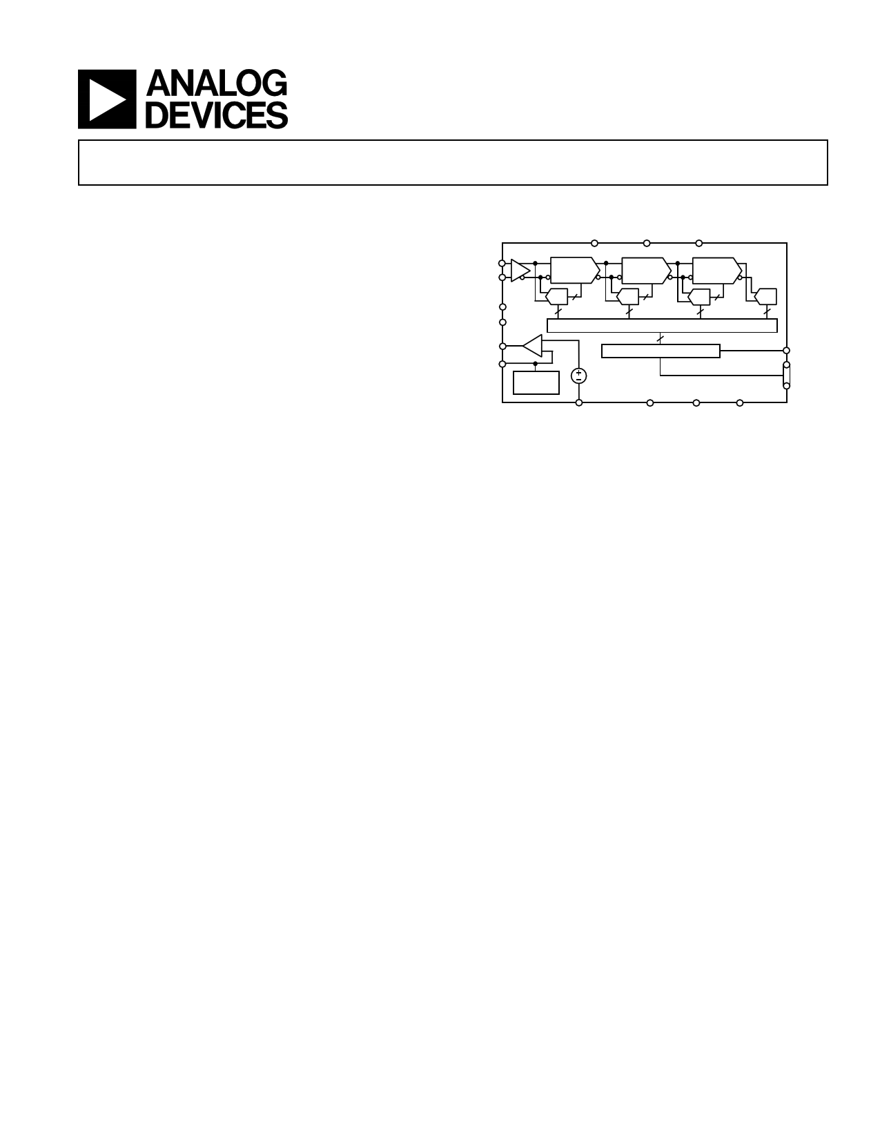
FUNCTIONAL BLOCK DIAGRAM
CLK
AVDD
DVDD
VINA
VINB
CAPT
CAPB
VREF
SENSE
SHA
MDAC1
GAIN = 16
MDAC2
GAIN = 8
MDAC3
GAIN = 4
5
A/D
4
A/D
3
A/D
54
3
DIGITAL CORRECTION LOGIC
12
OUTPUT BUFFERS
A/D
3
MODE
SELECT
1V
AD9221/AD9223/AD9220
REFCOM
AVSS
DVSS
CML
OTR
BIT 1
(MSB)
BIT 12
(LSB)
amplifier (SHA) is equally suited for both multiplexed sys-
tems that switch full-scale voltage levels in successive channels
as well as sampling single-channel inputs at frequencies up to
and beyond the Nyquist rate. Also, the AD9221/AD9223/AD9220
is well suited for communication systems employing Direct-
IF down conversion since the SHA in the differential input
mode can achieve excellent dynamic performance far beyond its
specified Nyquist frequency.2
A single clock input is used to control all internal conversion
cycles. The digital output data is presented in straight binary
output format. An out-of-range (OTR) signal indicates an over-
flow condition that can be used with the most significant bit to
determine low or high overflow.
PRODUCT HIGHLIGHTS
The AD9221/AD9223/AD9220 family offers a complete single-
chip sampling 12-bit, analog-to-digital conversion function in
pin compatible 28-lead SOIC and SSOP packages.
Flexible Sampling Rates—The AD9221, AD9223, and AD9220
offer sampling rates of 1.5 MSPS, 3.0 MSPS, and 10.0 MSPS,
respectively.
Low Power and Single Supply—The AD9221, AD9223, and
AD9220 consume only 59 mW, 100 mW, and 250 mW, respec-
tively, on a single 5 V power supply.
Excellent DC Performance Over Temperature—The AD9221/
AD9223/AD9220 provide 12-bit linearity and temperature drift
performance.1
Excellent AC Performance and Low Noise—The AD9221/
AD9223/AD9220 provide better than 11.3 ENOB performance
and have an input referred noise of 0.09 LSB rms.2
Flexible Analog Input Range—The versatile on-board sample-
and-hold (SHA) can be configured for either single-ended or
differential inputs of varying input spans.
One Technology Way, P.O. Box 9106, Norwood, MA 02062-9106, U.S.A.
Tel: 781/329-4700
www.analog.com
Fax: 781/326-8703 © 2003 Analog Devices, Inc. All rights reserved.
1 page 
PIN CONFIGURATION
CLK 1
28 DVDD
(LSB) BIT 12 2
27 DVSS
BIT 11 3
26 AVDD
BIT 10 4
BIT 9 5
BIT 8 6
AD9221/
AD9223/
AD9220
25 AVSS
24 VINB
23 VINA
BIT 7 7 TOP VIEW 22 CML
BIT 6 8 (Not to Scale) 21 CAPT
BIT 5 9
20 CAPB
BIT 4 10
19 REFCOM
BIT 3 11
18 VREF
BIT 2 12
17 SENSE
(MSB) BIT 1 13
16 AVSS
OTR 14
15 AVDD
PIN FUNCTION DESCRIPTIONS
Pin
Number
1
2
3–12
13
14
15, 26
16, 25
17
18
19
20
21
22
23
24
27
28
Mnemonic
CLK
BIT 12
BITS 11–2
BIT 1
OTR
AVDD
AVSS
SENSE
VREF
REFCOM
CAPB
CAPT
CML
VINA
VINB
DVSS
DVDD
Description
Clock Input Pin
Least Significant Data Bit (LSB)
Data Output Bit
Most Significant Data Bit (MSB)
Out of Range
5 V Analog Supply
Analog Ground
Reference Select
Reference I/O
Reference Common
Noise Reduction Pin
Noise Reduction Pin
Common-Mode Level (Midsupply)
Analog Input Pin (+)
Analog Input Pin (–)
Digital Ground
3 V to 5 V Digital Supply
DEFINITIONS OF SPECIFICATIONS
Integral Nonlinearity (INL)
INL refers to the deviation of each individual code from a line
drawn from “negative full scale” through “positive full scale.”
The point used as negative full scale occurs 1/2 LSB before the
first code transition. Positive full scale is defined as a level 1 1/2
LSB beyond the last code transition. The deviation is measured
from the middle of each particular code to the true straight line.
Differential Nonlinearity (DNL, No Missing Codes)
An ideal ADC exhibits code transitions that are exactly 1 LSB
apart. DNL is the deviation from this ideal value. Guaranteed
no missing codes to 12-bit resolution indicates that all 4096
codes, respectively, must be present over all operating ranges.
AD9221/AD9223/AD9220
Zero Error
The major carry transition should occur for an analog value 1/2
LSB below VINA = VINB. Zero error is defined as the devia-
tion of the actual transition from that point.
Gain Error
The first code transition should occur at an analog value 1/2 LSB
above negative full scale. The last transition should occur at an
analog value 1 1/2 LSB below the nominal full scale. Gain error
is the deviation of the actual difference between first and last
code transitions and the ideal difference between first and last
code transitions.
Temperature Drift
The temperature drift for zero error and gain error specifies the
maximum change from the initial (25°C) value to the value at
TMIN or TMAX.
Power Supply Rejection
The specification shows the maximum change in full scale from
the value with the supply at the minimum limit to the value with
the supply at its maximum limit.
Aperture Jitter
Aperture jitter is the variation in aperture delay for successive
samples and is manifested as noise on the input to the A/D.
Aperture Delay
Aperture delay is a measure of the sample-and-hold amplifier
(SHA) performance and is measured from the rising edge of the
clock input to when the input signal is held for conversion.
Signal-to-Noise and Distortion (S/N+D, SINAD) Ratio
S/N+D is the ratio of the rms value of the measured input signal
to the rms sum of all other spectral components below the Nyquist
frequency, including harmonics but excluding dc. The value for
S/N+D is expressed in decibels.
Effective Number of Bits (ENOB)
For a sine wave, SINAD can be expressed in terms of the num-
ber of bits. Using the following formula,
N = (SINAD – 1.76) / 6.02
it is possible to get a measure of performance expressed as N,
the effective number of bits.
Thus, effective number of bits for a device for sine wave inputs
at a given input frequency can be calculated directly from its
measured SINAD.
Total Harmonic Distortion (THD)
THD is the ratio of the rms sum of the first six harmonic com-
ponents to the rms value of the measured input signal and is
expressed as a percentage or in decibels.
Signal-to-Noise Ratio (SNR)
SNR is the ratio of the rms value of the measured input signal to
the rms sum of all other spectral components below the Nyquist
frequency, excluding the first six harmonics and dc. The value
for SNR is expressed in decibels.
Spurious Free Dynamic Range (SFDR)
SFDR is the difference in dB between the rms amplitude of the
input signal and the peak spurious signal.
REV. E
–5–
5 Page 
AD9221/AD9223/AD9220
Referring to Figure 5, the differential SHA is implemented using a
switched-capacitor topology. Therefore, its input impedance
and its subsequent effects on the input drive source should be
understood to maximize the converter’s performance. The com-
bination of the pin capacitance, CPIN, parasitic capacitance, CPAR,
and sampling capacitance, CS, is typically less than 16 pF.
When the SHA goes into track mode, the input source must
charge or discharge the voltage stored on CS to the new input
voltage. This action of charging and discharging CS, averaged
over a period of time and for a given sampling frequency, fS,
makes the input impedance appear to have a benign resistive
component. However, if this action is analyzed within a sampling
period (i.e., T = 1/fS), the input impedance is dynamic and there-
fore certain precautions on the input drive source should be
observed.
The resistive component to the input impedance can be com-
puted by calculating the average charge that gets drawn by CH
from the input drive source. It can be shown that if CS is allowed
to fully charge up to the input voltage before switches QS1 are
opened, then the average current into the input is the same as if
there were a resistor of 1/(CS fS) ohms connected between the
inputs. This means that the input impedance is inversely pro-
portional to the converter’s sample rate. Since CS is only 4 pF,
this resistive component is typically much larger than that of the
drive source (i.e., 25 kΩ at fS = 10 MSPS).
If one considers the SHA’s input impedance over a sampling
period, it appears as a dynamic input impedance to the input
drive source. When the SHA goes into the track mode, the input
source should ideally provide the charging current through RON
of switch QS1 in an exponential manner. The requirement of
exponential charging means that the most common input source,
an op amp, must exhibit a source impedance that is both low
and resistive up to and beyond the sampling frequency.
The output impedance of an op amp can be modeled with a
series inductor and resistor. When a capacitive load is switched
onto the output of the op amp, the output will momentarily
drop due to its effective output impedance. As the output recov-
ers, ringing may occur. To remedy the situation, a series resistor
can be inserted between the op amp and the SHA input as shown
in Figure 7. The series resistance helps isolate the op amp from
the switched-capacitor load.
VCC
AD9221/AD9223/
RS AD9220
VINA
RS
VINB
VEE
VREF
10F
0.1F
SENSE
REFCOM
Figure 7. Series Resistor Isolates Switched-Capacitor SHA
Input from Op Amp. Matching Resistors Improve SNR
Performance
The optimum size of this resistor is dependent on several factors,
which include the AD9221/AD9223/AD9220 sampling rate, the
selected op amp, and the particular application. In most applica-
tions, a 30 Ω to 50 Ω resistor is sufficient. However, some
applications may require a larger resistor value to reduce the noise
bandwidth or possibly limit the fault current in an overvoltage
condition. Other applications may require a larger resistor value
as part of an antialiasing filter. In any case, since the THD
performance is dependent on the series resistance and the above
mentioned factors, optimizing this resistor value for a given
application is encouraged.
A slight improvement in SNR performance and dc offset
performance is achieved by matching the input resistance of VINA
and VINB. The degree of improvement is dependent on the
resistor value and the sampling rate. For series resistor values
greater than 100 Ω, the use of a matching resistor is encouraged.
Figure 8 shows a plot for THD performance versus RSERIES for
the AD9221/AD9223/AD9220 at their respective sampling rate
and Nyquist frequency. The Nyquist frequency typically repre-
sents the worst case scenario for an ADC. In this case, a high
speed, high performance amplifier (AD8047) was used as the
buffer op amp. Although not shown, the AD9221/AD9223/AD9220
exhibits a slight increase in SNR (i.e. 1 dB to 1.5 dB) as the
resistance is increased from 0 kΩ to 2.56 kΩ due to its bandlimiting
effect on wideband noise. Conversely, it exhibits slight decrease
in SNR (i.e., 0.5 dB to 2 dB) if VINA and VINB do not have a
matched input resistance.
–45
–55
AD9223
–65
AD9220
–75
AD9221
–851
10 100
1k
RSERIES – ⍀
10k
Figure 8. THD vs. RSERIES (fIN = fS / 2, AIN = –0.5 dB, Input
Span = 2 V p-p, VCM = 2.5 V)
Figure 8 shows that a small RSERIES between 30 Ω and 50 Ω
provides the optimum THD performance for the AD9220.
Lower values of RSERIES are acceptable for the AD9223 and
AD9221 as their lower sampling rates provide a longer transient
recovery period for the AD8047. Note that op amps with lower
bandwidths will typically have a longer transient recovery period
and therefore require a slightly higher value of RSERIES and/or
lower sampling rate to achieve the optimum THD performance.
As the value of RSERIES increases, a corresponding increase in
distortion is noted. This is due to its interaction with the SHA’s
parasitic capacitor, CPAR, which has a signal dependency. Thus,
the resulting R-C time constant is signal dependent and conse-
quently a source of distortion.
The noise or small-signal bandwidth of the AD9221/AD9223/
AD9220 is the same as their full-power bandwidth as shown in
Figure 2. For noise sensitive applications, the excessive bandwidth
may be detrimental and the addition of a series resistor and/or
REV. E
–11–
11 Page | ||
| Páginas | Total 30 Páginas | |
| PDF Descargar | [ Datasheet AD9223.PDF ] | |
Hoja de datos destacado
| Número de pieza | Descripción | Fabricantes |
| AD9220 | Complete 12-Bit 1.5/3.0/10.0 MSPS Monolithic A/D Converters | Analog Devices |
| AD9221 | Monolithic A/D Converters | Analog Devices |
| AD9222 | 40/50 MSPS Serial LVDS 1.8 V A/D Converter | Analog Devices |
| AD9223 | Monolithic A/D Converters | Analog Devices |
| Número de pieza | Descripción | Fabricantes |
| SLA6805M | High Voltage 3 phase Motor Driver IC. |
Sanken |
| SDC1742 | 12- and 14-Bit Hybrid Synchro / Resolver-to-Digital Converters. |
Analog Devices |
|
DataSheet.es es una pagina web que funciona como un repositorio de manuales o hoja de datos de muchos de los productos más populares, |
| DataSheet.es | 2020 | Privacy Policy | Contacto | Buscar |