|
|
|
PDF AD9101 Data sheet ( Hoja de datos )
| Número de pieza | AD9101 | |
| Descripción | 125 MSPS Monolithic Sampling Amplifier | |
| Fabricantes | Analog Devices | |
| Logotipo | ||
Hay una vista previa y un enlace de descarga de AD9101 (archivo pdf) en la parte inferior de esta página. Total 12 Páginas | ||
|
No Preview Available !
a
125 MSPS Monolithic
Sampling Amplifier
AD9101
FEATURES
350 MHz Sampling Bandwidth
125 MHz Sampling Rate
Excellent Hold Mode Distortion
–75 dB @ 50 MSPS (25 MHz VIN)
–57 dB @ 125 MSPS (50 MHz VIN)
7 ns Acquisition Time to 0.1%
<1 ps Aperture Jitter
66 dB Feedthrough Rejection @ 50 MHz
3.3 nV/√Hz Spectral Noise Density
APPLICATIONS
Direct IF Sampling
Digital Sampling Oscilloscopes
HDTV Cameras
Peak Detectors
Radar/EW/ECM
Spectrum Analysis
Test Equipment/CCD Testers
DDS DAC Deglitcher
GENERAL DESCRIPTION
The AD9101 is an extremely accurate, general purpose, high
speed sampling amplifier. Its fast and accurate acquisition speed
allows for a wide range of frequency vs. resolution performance.
The AD9101 is capable of 8 to 12 bits of accuracy at clock rates
of 125 MSPS or 50 MSPS, respectively. This level of perfor-
mance makes it an ideal driver for almost all 8- to 12-bit A/D
encoders on the market today.
In effect, the AD9101 is a track-and-hold with a post amplifier.
This configuration allows the front end sampler to operate at
relatively low signal amplitudes. This results in dramatic im-
provement in both track and hold mode distortion while keeping
power low.
The gain-of-four output amplifier has been optimized for fast
and accurate large signal step settling characteristics even when
heavily loaded. This amplifier’s fast Settling Time Linearity
(STL) characteristic causes the amplifier to be transparent to
the low signal level distortion of the sampler. When sampled,
output distortion levels reflect only the distortion performance
of the sampler.
Dramatic SNR and distortion improvements can be realized
when using the AD9101 with high speed flash converters. Flash
converters generally have excellent linearity at dc and low fre-
quencies. However, as signal slew rate increases, their perfor-
mance degrades due to the internal comparators’ aperture delay
variations and finite gain bandwidth product.
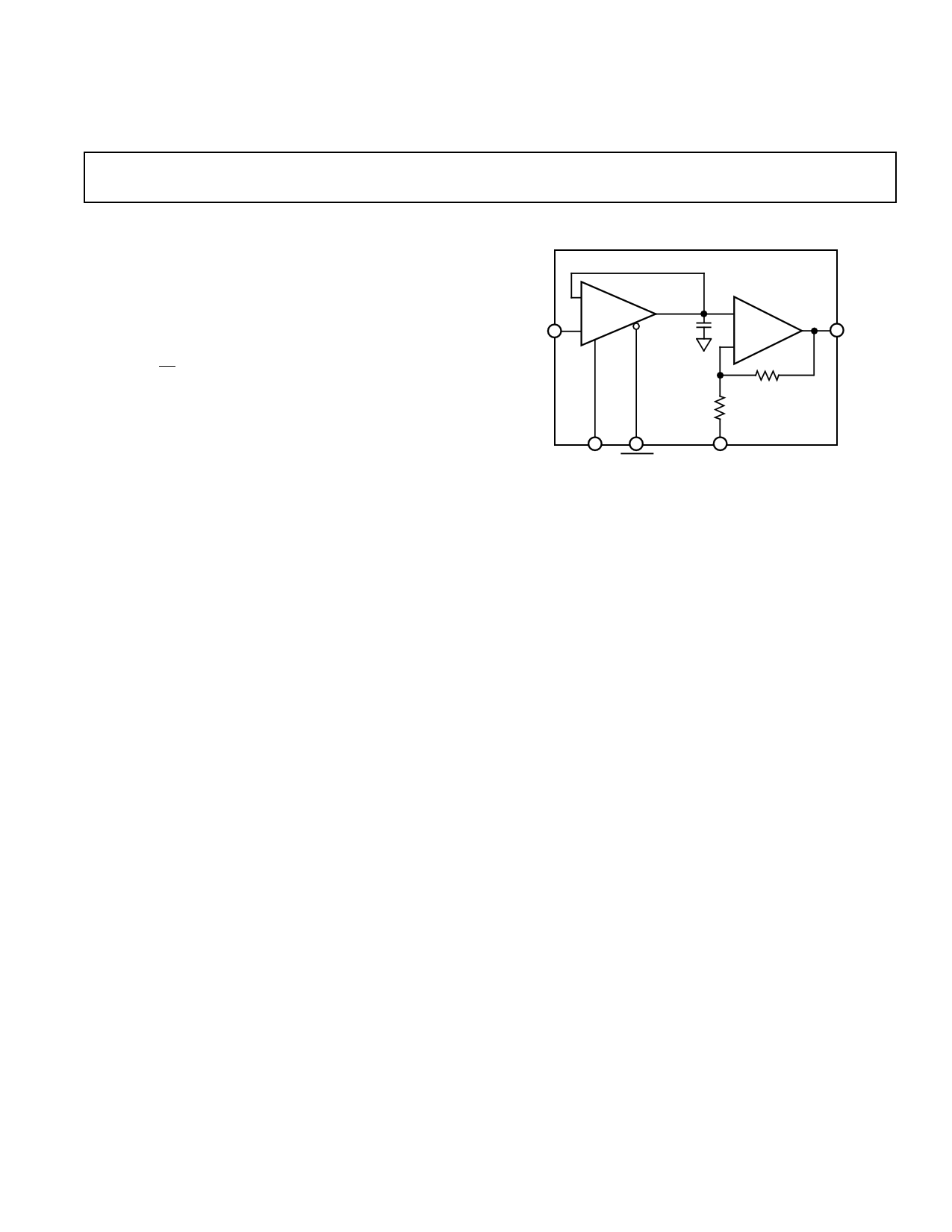
FUNCTIONAL BLOCK DIAGRAM
–
SAMPLER
VIN +
CHOLD
AD9101
+
4X
AMP
–
VOUT
3R
R
CLOCK CLOCK
RTN
The benefits of using a track-and-hold ahead of a flash converter
have been well known for many years. However, before the
AD9101, there was no track-and-hold amplifier with sufficient
bandwidth and linearity to markedly increase the dynamic per-
formance of such flashes as the AD9002, AD9012, AD9020,
and AD9060.
A new application made possible by the AD9101 is direct IF-
to-digital conversion. Utilizing the Nyquist principle, the IF
frequency can be rejected, and the baseband signal can be
recovered. As an example, a 40 MHz IF is modulated by a
10 MHz bandwidth signal. By sampling at 25 MSPS, the signal
of interest is detected.
The AD9101 is offered in commercial and military temperature
ranges. Commercial versions include the AD9101AR in plastic
SOIC and AD9101AE in ceramic LCC. Military devices are
available in ceramic LCC. Contact the factory for availability of
versions in DIP and/or military versions.
PRODUCT HIGHLIGHTS
1. Guaranteed Hold-Mode Distortion
2. 125 MHz Sampling Rate to 8 Bits; 50 MHz to 12 Bits
3. 350 MHz Sampling Bandwidth
4. Super-Nyquist Sampling Capability
5. Output Offset Adjustable
REV. 0
Information furnished by Analog Devices is believed to be accurate and
reliable. However, no responsibility is assumed by Analog Devices for its
use, nor for any infringements of patents or other rights of third parties
which may result from its use. No license is granted by implication or
otherwise under any patent or patent rights of Analog Devices.
One Technology Way, P.O. Box 9106, Norwood, MA 02062-9106, U.S.A.
Tel: 617/329-4700
Fax: 617/326-8703
1 page 
AD9101
THEORY OF OPERATION
The AD9101 employs a new and unique track-and-hold archi-
tecture. Previous commercially available high speed track-and-
holds used an open loop input buffer, followed by a diode
bridge, hold capacitor, and output buffer (closed or open loop)
with a FET device usually connected to the hold capacitor. This
architecture required mixed device technology and, usually, hy-
brid construction. The sampling rate of these hybrids has been
limited to 20 MSPS for 12-bit accuracy. Distortion generated in
the front-end amplifier/bridge limited the dynamic range perfor-
mance to the “mid –70 dBFS” for analog input signals of less
than 10 MHz. Broadband and switch-generated noise limited
the SNR of previous track-and-holds to about 70 dB.
The AD9101 is a monolithic device using a high frequency
complementary bipolar process to achieve new levels of high
speed precision. Its architecture completely breaks from the tra-
ditional architecture described above. The hold switch has been
integrated into the first stage closed-loop buffer. This innova-
tion provides error (distortion) correction for both the switch
and buffer while still achieving slew rates representative of an
open-loop design. In addition, acquisition slew current for the
hold capacitor is higher than the traditional diode bridge switch
configurations, removing a main contributor to the limits of
maximum sampling rate, input frequency, and distortion.
The closed-loop output amplifier includes zero voltage bias cur-
rent cancellation, which results in high-temperature droop rates
close to those found in FET type inputs. This closed-loop am-
plifier inherently provides high speed loop correction and has
extremely low distortion even when heavily loaded.
Extremely fast time constant linearity (7 ns to 0.01% for a 4 V
output step) ensures that the output amplifier does not limit the
AD9101 sampling rate or analog input frequency. (The acquisi-
tion and settling time are primarily limited only by the input
sampler.) The output is transparent to the overall AD9101 hold
mode distortion levels for loads as low as 50 Ω.
Full-scale track and acquisition slew rates achieved by the
AD9101 are 1800 V/µs and 1700 V/µs, respectively. When com-
bined with excellent phase margin (typically 5% overshoot),
wide bandwidth, and dc gain accuracy, acquisition time to
0.01% is only 11 ns.
Acquisition Time
Acquisition time is the amount of time it takes the AD9101 to
reacquire the analog input when switching from hold-to-track
mode. The interval starts at the 50% clock transition point and
ends when the input signal is reacquired to within a specified er-
ror band at the hold capacitor.
The hold-to-track switch delay (tDHT) cannot be subtracted
from this acquisition time for 12-bit performance because it is a
charging time and analog output delay that occurs when moving
from hold to track; this delay is typically 1.5 ns. Therefore, the
track time required for the AD9101 is the acquisition time
which includes tDHT. Note that the acquisition time is defined as
the settled voltage at the hold capacitor and does not include the
delay and settling time of the output amplifier. The example in
Figure 1 illustrates why the output amplifier does not contribute
to the overall acquisition time.
The exaggerated illustration in Figure 1 shows that VHC has
settled to within x% of its final value, but VOUT (due to slew rate
limitations, finite BW, power supply ringing, etc.) has not settled
VHC
SAMPLER
HC
VOUT
AMP
TRACK-TO-HOLD
INDUCED GLITCH
VHC
VOUT
tDHT
1.5ns
ACQUISITION TIME
AT HC TO X%
TRACK
TS
HOLD
Figure 1. Acquisition Time at Hold Capacitor
during the track time. However, since the output amplifier al-
ways “tracks” the front end circuitry, it “catches up” and di-
rectly superimposes itself (less about 500 ps of analog delay) to
VHC. Since the small signal settling time of the output amplifier
can be about 1.2 ns to ± 1 mV, and is significantly less than the
hold time, acquisition time should be referenced to the hold
capacitor.
Most of the hold settling time and output acquisition time are
due to the sampler and the switch network. (Output acquisition
time is as seen on a scope at the output. This is typically 1.7 ns
longer than actual acquisition time.) For track time, the output
amplifier contributes only about 5 ns of the total; in hold mode,
it contributes 1.7 ns (as stated above).
A stricter definition of acquisition would actually include both
the acquisition and track-to-hold settling times to a defined ac-
curacy. To obtain 12-bit+ distortion levels and 50 MSPS opera-
tion, the minimum recommended track and hold times are
12 ns and 8 ns, respectively. To drive an 8-bit flash converter
(such as the AD9002) with a 2 V p-p full-scale input, hold time
to 1 LSB accuracy will be limited primarily by the aperture time
of the encoder, rather than by the AD9101. This makes it pos-
sible to reduce track time to as little as 5 ns, with hold time cho-
sen to optimize the encoder’s performance.
Though acquisition time and track-to-hold settling time to
1/2 LSB (0.4%) accuracy are 6 ns and 4 ns respectively, it is still
possible to achieve –45 dB SNR performance at clock speeds to
125 MSPS. This is because the settling error is roughly propor-
tional to the signal level and is partially cancelled due to the
high phase margin of the input sampler.
Hold vs. Track Mode Distortion
In many traditional high speed, open-loop track-and-holds,
track mode distortion is often much better than hold mode dis-
tortion. Track mode distortion does not include nonlinearities
due to the switch network, and does not correlate to the relevant
hold mode distortion. But since hold mode distortion has tradi-
tionally been omitted from manufacturer’s specification tables,
users have had to discover for themselves the effective overall
hold mode distortion of the combined T/H and encoder.
REV. 0
–5–
5 Page 
OUTLINE DIMENSIONS
Dimensions are shown in inches and (mm).
AD9101
20-Pin SOIC
0.512 (13.00)
0.496 (12.60)
20
TOP VIEW
1
11
0.299 (7.60)
0.291 (7.40)
0.419 (10.65)
0.394 (10.00)
10
0.50 (1.27) BSC 0.019 (0.49)
0.014 (0.35)
0.0125 (0.32)
0.0091 (0.23)
0.104 (2.65)
0.093 (2.35)
0.012 (0.30)
0.004 (0.10)
0.050 (1.27)
0.016 (0.40)
20-Contact LCC
0.055 (1.40)
0.045 (1.14)
19 20 1 2 3
18
NO. 1 PIN
17 INDEX
16 BOTTOM VIEW
15
14
4
5
6
7
8
13 12 11 10 9
0.075
(1.91)
REF.
0.028 (0.71)
0.022 (0.56)
0.050
(1.27)
BSC
0.358 (9.09)
0.342 (8.69)
0.100 (2.54)
0.064 (1.63)
REV. 0
–11–
11 Page | ||
| Páginas | Total 12 Páginas | |
| PDF Descargar | [ Datasheet AD9101.PDF ] | |
Hoja de datos destacado
| Número de pieza | Descripción | Fabricantes |
| AD9100 | Ultrahigh Speed Monolithic Track-and-Hold | Analog Devices |
| AD9101 | 125 MSPS Monolithic Sampling Amplifier | Analog Devices |
| AD9102 | Digital to Analog Converter and Waveform Generator | Analog Devices |
| AD9106 | Digital-to-Analog Converter and Waveform Generator | Analog Devices |
| Número de pieza | Descripción | Fabricantes |
| SLA6805M | High Voltage 3 phase Motor Driver IC. |
Sanken |
| SDC1742 | 12- and 14-Bit Hybrid Synchro / Resolver-to-Digital Converters. |
Analog Devices |
|
DataSheet.es es una pagina web que funciona como un repositorio de manuales o hoja de datos de muchos de los productos más populares, |
| DataSheet.es | 2020 | Privacy Policy | Contacto | Buscar |