|
|
|
PDF AD9066 Data sheet ( Hoja de datos )
| Número de pieza | AD9066 | |
| Descripción | Dual 6-Bit/ 60 MSPS Monolithic A/D Converter | |
| Fabricantes | Analog Devices | |
| Logotipo | ||
Hay una vista previa y un enlace de descarga de AD9066 (archivo pdf) en la parte inferior de esta página. Total 7 Páginas | ||
|
No Preview Available !
a
FEATURES
Two Matched ADCs on Single Chip
CMOS-Compatible I/O
Low-Power (400 mW) Dissipation
Single +5 V Supply
On-Chip Voltage Reference
Self-Biased for AC-Coupled Inputs
28-Lead SOIC and SSOP Packages
APPLICATIONS
Direct Broadcast Satellite (DBS) Receivers
QAM Demodulators
Wireless LANs
VSAT Receivers
Dual 6-Bit, 60 MSPS
Monolithic A/D Converter
AD9066
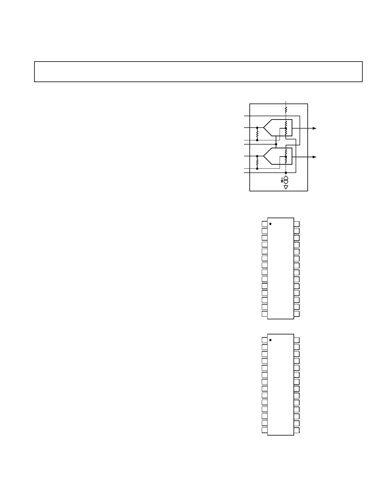
FUNCTIONAL BLOCK DIAGRAM
+VS
AD9066
VT
INA
6-BIT
DAC
D0A-D5A
REF A
ENCODE
INB
6-BIT
DAC
D0B-D5B
REF B
VB
PRODUCT DESCRIPTION
The AD9066 is a dual 6-bit ADC that has been optimized for
low-cost in-phase and quadrature (I and Q) demodulators.
Primary applications include digital direct broadcast satellite
applications where broadband quadrature phase shift keying
(QPSK) modulation is used. In these receivers the recovered signal
is separated into I and Q vector components and digitized.
To reduce total system cost and power dissipation, the AD9066
provides an internal voltage reference and operates from a
single +5 volt power supply. Digital outputs are CMOS com-
patible and rated to 60 MSPS conversion rates. The digital
input (ENCODE) utilizes a CMOS input stage with a TTL
compatible (1.4 V) threshold.
The AD9066 is housed in a 28-lead SOIC and a 28-lead SSOP
package and is available in two temperature grades. The
AD9066JR is rated for operation over the 0°C to 70°C commer-
cial temperature range. The AD9066AR/ARS is rated for the
–40°C to +85°C industrial temperature range.
The internal voltage reference insures that the analog input is
biased to midscale with low offset when driven from an ac-
coupled source. In dc-coupled applications, the midscale voltage
reference can be used to control external biasing amplifiers to
minimize offsets due to variations in temperature or supply voltage.
REV. A
Information furnished by Analog Devices is believed to be accurate and
reliable. However, no responsibility is assumed by Analog Devices for its
use, nor for any infringements of patents or other rights of third parties
which may result from its use. No license is granted by implication or
otherwise under any patent or patent rights of Analog Devices.
PIN CONFIGURATIONS
ENCODE 1
28 D5A (MSB)
+VS 2
GND 3
27 D4A
26 D3A
GND 4
25 D2A
+VS 5
INA 6
AD9066
(JR/AR)
24 D1A
23 D0A (LSB)
GND 7 TOP VIEW 22 GND
+VS 8 (Not to Scale) 21 +VS
VT 9
20 D5B (MSB)
REF A 10
19 D4B
INB 11
18 D3B
REF B 12
17 D2B
VB 13
16 D1B
NC 14
15 D0B (LSB)
NC = NO CONNECT
+VS 1
28 GND
VT 2
27 INA
REF A 3
INB 4
26 +VS
25 GND
REF B 5
24 GND
VB 6
AD9066
(ARS)
23 +VS
NC 7 TOP VIEW 22 ENCODE
(LSB) D0B 8 (Not to Scale) 21 D5A (MSB)
D1B 9
20 D4A
D2B 10
19 D3A
D3B 11
18 D2A
D4B 12
17 D1A
(MSB) D5B 13
16 D0A (LSB)
+VS 14
15 GND
NC = NO CONNECT
One Technology Way, P.O. Box 9106, Norwood, MA 02062-9106, U.S.A.
Tel: 781/329-4700 World Wide Web Site: http://www.analog.com
Fax: 781/326-8703
© Analog Devices, Inc., 2000
1 page 
AD9066
Timing
The duty cycle of the encode clock for the AD9066 is critical in
obtaining rated performance of the ADC. Rated maximum and
minimum pulse widths should be maintained, especially for
sample rates greater than 40 MSPS.
The AD9066 provides latched data outputs with three pipeline
delays. The length and load on the output data lines should be
minimized to reduce power supply transients inside the AD9066
which might diminish dynamic performance.
ANALOG
INPUT
N
tA
N+1
N+2
ENCODE
tV
D0–D5
VALID DATA
FOR N–3
tPD
VALID DATA
FOR N–2
VALID DATA
FOR N–1
DATA
CHANGING
Figure 5. Timing Diagram
The data is invalid during the period between tV and tPD. This
period refers to the time required for the AD9066 to fully switch
between valid CMOS logic levels. When latching the output
data, be careful to observe latch setup and hold time restrictions
as well as this data invalid period when designing the system
timing.
Layout and Signal Care
To insure optimum performance, a single low impedance
ground plane is recommended. Analog and digital grounds
should be connected together at the AD9066. Analog and digi-
tal power supplies should be bypassed, at the device, to ground
through 0.1 µF ceramic capacitors.
The use of sockets may limit the dynamic performance of the
part and is not recommended except for prototype or evaluation
purposes.
Driving the AD9066 with a Bipolar Input
The analog input range of the AD9066 is between 3.7 V and
4.2 V. Because the input is offset, the normal method of driving
the analog input is to use a blocking capacitor between the ana-
log source and the AD9066 analog input pins. In applications
where DC coupling must be employed, the simple circuit shown
in Figure 6 will take a bipolar input and offset it to the operating
range of the AD9066.
To offset the input, the midpoint voltage of the AD9066 is buff-
ered off chip and then inverted with an AD712, a low input bias
current dual op amp. This inverted midpoint is then fed to a
summation amplifier that combines the bipolar input with the
inverted offset voltage. The summation amplifier is an AD812, a
wideband current feedback amplifier that provides good band-
width and low distortion.
866⍀
866⍀
866⍀
ENCODE
+ 1/2
AD812
2k⍀
1/2
AD712
2k⍀
INA
AD9066
REF A
OR REF B
6 BITS
866⍀
866⍀
+
1/2
AD712
866⍀
+15V
6 BITS
+ 1/2
AD812
–15V
INB
Figure 6. Bipolar Input Using AD812 Drive for AD9066
Layout should follow high frequency/high speed design guide-
lines. In addition the capacitance around the inverting input to
the AD812 should be minimized through a tight layout and the
use of low capacitance chip resistors for gain setting.
Quadrature Receiver Using the AD9066
Although any type of input signal may be applied, the AD9066
has been optimized for low cost in-phase and quadrature (I and
Q) demodulators. Primary applications include digital direct
broadcast satellite applications where broadband quadrature
phase shift keying (QPSK) modulation is used. In these receivers
the recovered signal is separated into I and Q vector components
and digitized.
IF IN
90؇
AD9066
LPF ADC
LPF ADC
VCO
VCO
Figure 7. Simplified Block Diagram
For data symbol rates less than 10 Mbaud, the AD607 IF/RF
receiver subsystem provides an ideal solution for the second
conversion stage of a complete receiver system. Figure 8 shows
the AD9066 and AD607 used together.
The AD607 accepts inputs as high as 500 MHz which may be
the output of the first IF stage or RF signals directly. The IF/RF
signal is mixed with the local oscillator to provide an IF fre-
quency of 400 kHz to 22 MHz. This signal is filtered externally
and then amplified with an on-chip AGC before being synchro-
nously demodulated with an on-chip PLL carrier recovery
circuit. The outputs are digitized with the AD9066. The digital
outputs may be processed with a DSP chip such as the ADSP-
2171, ADSP-21062, general purpose DSP or ASIC.
REV. A
–5–
5 Page | ||
| Páginas | Total 7 Páginas | |
| PDF Descargar | [ Datasheet AD9066.PDF ] | |
Hoja de datos destacado
| Número de pieza | Descripción | Fabricantes |
| AD9060 | 10-Bit 75 MSPS A/D Converter | Analog Devices |
| AD9066 | Dual 6-Bit/ 60 MSPS Monolithic A/D Converter | Analog Devices |
| Número de pieza | Descripción | Fabricantes |
| SLA6805M | High Voltage 3 phase Motor Driver IC. |
Sanken |
| SDC1742 | 12- and 14-Bit Hybrid Synchro / Resolver-to-Digital Converters. |
Analog Devices |
|
DataSheet.es es una pagina web que funciona como un repositorio de manuales o hoja de datos de muchos de los productos más populares, |
| DataSheet.es | 2020 | Privacy Policy | Contacto | Buscar |