|
|
|
PDF AD8323 Data sheet ( Hoja de datos )
| Número de pieza | AD8323 | |
| Descripción | 5 V CATV Line Driver Fine Step Output Power Control | |
| Fabricantes | Analog Devices | |
| Logotipo | ||
Hay una vista previa y un enlace de descarga de AD8323 (archivo pdf) en la parte inferior de esta página. Total 16 Páginas | ||
|
No Preview Available !
a
FEATURES
Supports DOCSIS Standard for Reverse Path
Transmission
Gain Programmable in 0.75 dB Steps Over a 53.5 dB
Range
Low Distortion at 60 dBmV Output
–56 dBc SFDR at 21 MHz
–55 dBc SFDR at 42 MHz
Output Noise Level
–48 dBmV in 160 kHz
Maintains 75 ⍀ Output Impedance
Power-Up and Power-Down Condition
Upper Bandwidth: 100 MHz (Full Gain Range)
5 V Supply Operation
Supports SPI Interfaces
APPLICATIONS
Gain-Programmable Line Driver
HFC High-Speed Data Modems
Interactive Set-Top Boxes
PC Plug-in Modems
General-Purpose Digitally Controlled Variable Gain Block
5 V CATV Line Driver Fine Step
Output Power Control
AD8323
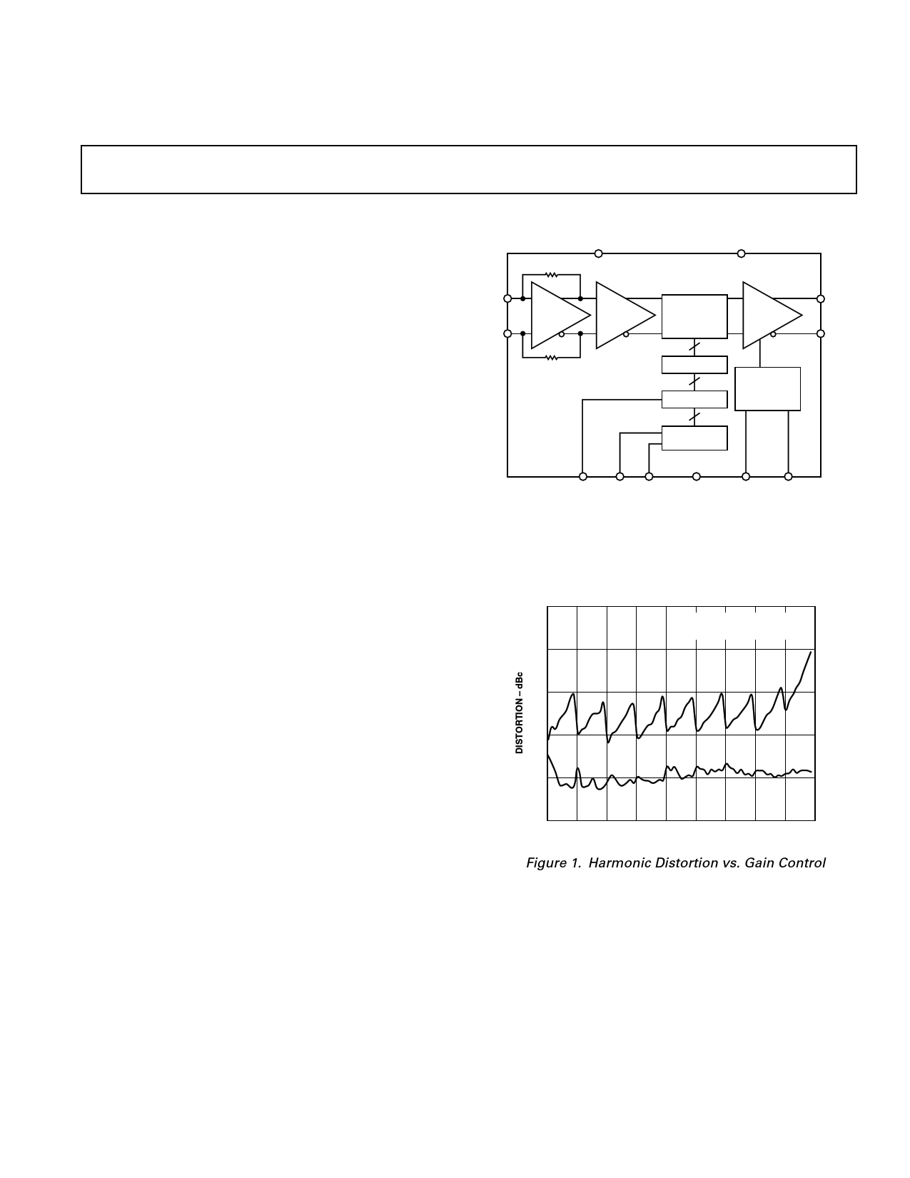
FUNCTIONAL BLOCK DIAGRAM
VCC (7 PINS)
R1
VIN+
VIN–
DIFF OR
SINGLE
INPUT
AMP
BUFFER
R2
ZIN (SINGLE) = 800⍀
ZIN (DIFF) = 1.6k⍀
BYP
AD8323
ATTENUATION
CORE
8
DECODE
POWER
AMP
ZOUT DIFF =
75⍀
VOUT+
VOUT–
8
DATA LATCH
POWER-DOWN
LOGIC
8
SHIFT
REGISTER
DATEN DATA CLK GND (11 PINS) PD
SLEEP
GENERAL DESCRIPTION
The AD8323 is a low-cost, digitally controlled, variable gain ampli-
fier optimized for coaxial line driving applications such as cable
modems that are designed to the MCNS-DOCSIS upstream
standard. An 8-bit serial word determines the desired output gain
over a 53.5 dB range resulting in gain changes of 0.7526 dB/LSB.
The AD8323 comprises a digitally controlled variable attenuator
of 0 dB to –53.5 dB, which is preceded by a low noise, fixed
gain buffer and is followed by a low distortion high power am-
plifier. The AD8323 accepts a differential or single-ended input
signal. The output is specified for driving a 75 Ω load, such as
coaxial cable.
Distortion performance of –56 dBc is achieved with an output
level up to 60 dBmV at 21 MHz bandwidth. A key performance
and cost advantage of the AD8323 results from the ability to main-
tain a constant 75 Ω output impedance during power-up and
power-down conditions. This eliminates the need for external 75 Ω
termination, resulting in twice the effective output voltage when
compared to a standard operational amplifier. In addition, this
device has a sleep mode function that reduces the quiescent
current to 4 mA.
The AD8323 is packaged in a low-cost 28-lead TSSOP, operates
from a single 5 V supply, and has an operational temperature
range of –40°C to +85°C.
–50
FO = 42MHz
PO = 60dBmV @ MAX GAIN
–55
–60 HD3
–65
HD2
–70
–75
0
8 16 24 32 40 48 56 64 72
GAIN CONTROL – DEC Code
Figure 1. Harmonic Distortion vs. Gain Control
REV. 0
Information furnished by Analog Devices is believed to be accurate and
reliable. However, no responsibility is assumed by Analog Devices for its
use, nor for any infringements of patents or other rights of third parties
which may result from its use. No license is granted by implication or
otherwise under any patent or patent rights of Analog Devices.
One Technology Way, P.O. Box 9106, Norwood, MA 02062-9106, U.S.A.
Tel: 781/329-4700 World Wide Web Site: http://www.analog.com
Fax: 781/326-8703
© Analog Devices, Inc., 2000
1 page 
Typical Performance Characteristics–AD8323
VCC TOKO 617DB–A0070
1:1
VIN
RTI
0.1F
82.5⍀
VIN–
0.1F
OUT–
OUT
RL 75⍀
0.1F
OUT+
VIN+ GND
39.2⍀
0.1F
34
IN
31
28
25
22
VIN –
VIN+
1:1 OUT
POUT = 60dBmV
@ MAX GAIN
CL
RL 75⍀
CL = 0pF
CL = 50pF
CL = 20pF
CL = 10pF
TPC 1. Basic Test Circuit
19
1 10 100
FREQUENCY – MHz
TPC 4. AC Response for Various Cap Loads
1.5
1.0
0.5 f = 10MHz
0.0 f = 5MHz
f = 42MHz
–0.5
–1.0
f = 65MHz
–1.5
0 8 16 24 32 40 48 56 64
GAIN CONTROL – Decimal
TPC 2. Gain Error vs. Gain Control
72
–30
f = 10MHz
PD = 1
–34
–38
–42
–46
–50
0
8 16 24 32 40 48 56 64 72
GAIN CONTROL – Decimal
TPC 5. Output Referred Noise vs. Gain Control
40
30
20
10
0
–10
–20
–30
–40
0.1
71D
46D
23D
00D
1 10 100
FREQUENCY – MHz
TPC 3. AC Response
1k
0
PD = 0
VIN = 116mV p-p
–20
MAX GAIN
–40
–60
MIN GAIN
–80
–100
0.1
1 10 100
FREQUENCY – MHz
1k
TPC 6. Input Signal Feedthrough vs. Frequency
REV. 0
–5–
5 Page 
EVALUATION BOARD FEATURES AND OPERATION
AD8323
Figure 9. Screen Display of Windows-Based Control Software
REV. 0
–11–
11 Page | ||
| Páginas | Total 16 Páginas | |
| PDF Descargar | [ Datasheet AD8323.PDF ] | |
Hoja de datos destacado
| Número de pieza | Descripción | Fabricantes |
| AD8320 | Serial Digital Controlled Variable Gain Line Driver | Analog Devices |
| AD8321 | Gain Programmable CATV Line Driver | Analog Devices |
| AD8322 | 5 V CATV Line Driver Coarse Step Output Power Control | Analog Devices |
| AD8323 | 5 V CATV Line Driver Fine Step Output Power Control | Analog Devices |
| Número de pieza | Descripción | Fabricantes |
| SLA6805M | High Voltage 3 phase Motor Driver IC. |
Sanken |
| SDC1742 | 12- and 14-Bit Hybrid Synchro / Resolver-to-Digital Converters. |
Analog Devices |
|
DataSheet.es es una pagina web que funciona como un repositorio de manuales o hoja de datos de muchos de los productos más populares, |
| DataSheet.es | 2020 | Privacy Policy | Contacto | Buscar |