|
|
|
PDF ADP3422JRU Data sheet ( Hoja de datos )
| Número de pieza | ADP3422JRU | |
| Descripción | IMVP-II-Compliant Core Power Controller for Mobile CPUs | |
| Fabricantes | Analog Devices | |
| Logotipo | ||
Hay una vista previa y un enlace de descarga de ADP3422JRU (archivo pdf) en la parte inferior de esta página. Total 16 Páginas | ||
|
No Preview Available !
a IMVP-II-Compliant
Core Power Controller for Mobile CPUs
ADP3422
FEATURES
Certified IMVP-II Controller
Excellent Transient Containment
Minimum Number of Output Capacitors
Fast, Smooth, Output Transition During VID Code Change
Current Limit with Hiccup Protection
Transient-Glitch-Free Power Good
Low Shutdown Current
Soft Start Eliminates In-Rush Current Surge
Adaptive Noise-Blanking Enhancement for Speed and
Stability
Highly Redundant Over-Voltage and Reverse-Voltage
Protection
Controls Synchronous Rectifier for Improved Battery Life
APPLICATIONS
IMVP-II Enabled Core DC/DC Converters
Fixed-Voltage Mobile CPU Core DC/DC Converters
Notebook/Laptop Power Supplies
Programmable Output Power Supplies
GENERAL DESCRIPTION
The ADP3422 is a hysteretic dc-dc buck converter controller to
power a mobile processor’s core. The optimized low voltage
design is powered from the 3.3 V system supply. The output
voltage is set by a 5-bit VID code. To accommodate the transition
time required by the newest processors for on-the-fly VID
changes, the ADP3422 features high-speed operation to allow a
minimized inductor size that results in the fastest change of
current to the output. To further allow for the minimum number
of output capacitors to be used, the ADP3422 features active
voltage positioning that can be optimally compensated to ensure a
superior load transient response. The output signal interfaces
with the ADP3415 MOSFET driver that is optimized for high
speed and high efficiency for driving both the upper and lower
(synchronous) MOSFETs of the buck converter.
HYSSET
CPUSET
FSHIFT
DSHIFT
BSHIFT
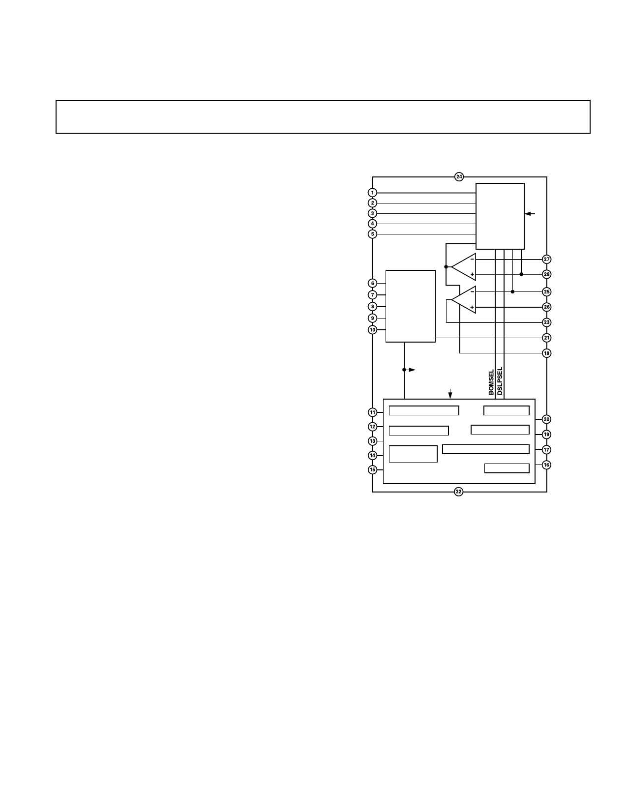
FUNCTIONAL BLOCK DIAGRAM
ADP3422
VCC
HYSTERESIS
AND
SHIFT-SETTING
VR
VID4
VID3
VID2
VID1
VID0
CLIM
PROGRAMMED
DAC
AND
FIXED
REFERENCE
EN
CORE
VR
VCC
CS+
CS–
RAMP
REG
OUT
DACOUT
SWFB
BOM
DSLP
DPRSLP
PWRGD
SD
UVLO AND MAIN BIAS
SR CONTROL
PWRGD BLANKER
PWRGD MONITOR
OP MODE
SELECTOR
SS-HICCUP TIMER AND OCP
OVP AND RVP
POWER MANAGEMENT
COREFB
SS
DRVLSD
CLAMP
GND
REV. 0
Information furnished by Analog Devices is believed to be accurate and
reliable. However, no responsibility is assumed by Analog Devices for its
use, nor for any infringements of patents or other rights of third parties that
may result from its use. No license is granted by implication or otherwise
under any patent or patent rights of Analog Devices.
One Technology Way, P.O. Box 9106, Norwood, MA 02062-9106, U.S.A.
Tel: 781/329-4700
www.analog.com
Fax: 781/326-8703
© Analog Devices, Inc., 2001
1 page 
ABSOLUTE MAXIMUM RATINGS*
Input Supply Voltage (VCC) . . . . . . . . . . . . . . –0.3 V to +7 V
UVLO Input Voltage . . . . . . . . . . . . . . . . . . . . –0.3 V to +7 V
All Other Inputs/Outputs . . . . . . . . . –0.3 V to (VCC + 0.3 V)
Operating Ambient Temperature Range . . . . . . . 0°C to 85°C
Junction Temperature Range . . . . . . . . . . . . . . . 0°C to 150°C
θJA . . . . . . . . . . . . . . . . . . . . . . . . . . . . . . . . . . . . . . . 98°C/W
Storage Temperature Range . . . . . . . . . . . . –65°C to +150°C
Lead Temperature (Soldering, 10 sec) . . . . . . . . . . . . 300°C
*This is a stress rating only; operation beyond these limits can cause the device to
be permanently damaged.
ORDERING GUIDE
Model
Temperature Package
Range
Description
Package
Option
ADP3422JRU 0°C to 85°C Thin Shrink Small RU-28
Outline (TSSOP)
ADP3422
PIN CONFIGURATION
HYSSET 1
28 CS–
CPUSET 2
27 CS+
FSHIFT 3
26 REG
DSHIFT 4
25 RAMP
BSHIFT 5
24 VCC
VID4 (MSB)
VID3
VID2
6 23
ADP3422
7 TOP VIEW 22
8
(Not to Scale)
21
OUT
GND
DACOUT
VID1 9
20 COREFB
VID0 (LSB) 10
19 SS
BOM 11
DSLP 12
18 SWFB
17 DRVLSD
DPRSLP 13
PWRGD 14
16 CLAMP
15 SD
CAUTION
ESD (electrostatic discharge) sensitive device. Electrostatic charges as high as 4000 V readily
accumulate on the human body and test equipment and can discharge without detection. Although
the ADP3422 features proprietary ESD protection circuitry, permanent damage may occur on
devices subjected to high-energy electrostatic discharges. Therefore, proper ESD precautions are
recommended to avoid performance degradation or loss of functionality.
WARNING!
ESD SENSITIVE DEVICE
REV. 0
–5–
5 Page 
ADP3422
REV. 0
Figure 3. Application Circuit
–11–
11 Page | ||
| Páginas | Total 16 Páginas | |
| PDF Descargar | [ Datasheet ADP3422JRU.PDF ] | |
Hoja de datos destacado
| Número de pieza | Descripción | Fabricantes |
| ADP3422JRU | IMVP-II-Compliant Core Power Controller for Mobile CPUs | Analog Devices |
| Número de pieza | Descripción | Fabricantes |
| SLA6805M | High Voltage 3 phase Motor Driver IC. |
Sanken |
| SDC1742 | 12- and 14-Bit Hybrid Synchro / Resolver-to-Digital Converters. |
Analog Devices |
|
DataSheet.es es una pagina web que funciona como un repositorio de manuales o hoja de datos de muchos de los productos más populares, |
| DataSheet.es | 2020 | Privacy Policy | Contacto | Buscar |