|
|
|
PDF ADP3300 Data sheet ( Hoja de datos )
| Número de pieza | ADP3300 | |
| Descripción | High Accuracy anyCAP 50 mA Low Dropout Linear Regulator | |
| Fabricantes | Analog Devices | |
| Logotipo | ||
Hay una vista previa y un enlace de descarga de ADP3300 (archivo pdf) en la parte inferior de esta página. Total 8 Páginas | ||
|
No Preview Available !
a
High Accuracy anyCAP®
50 mA Low Dropout Linear Regulator
ADP3300
FEATURES
High Accuracy (Over Line and Load Regulations
at 25؇C): ؎0.8%
Ultralow Dropout Voltage: 80 mV Typical @ 50 mA
Requires Only CO = 0.47 F for Stability
anyCAP™ = Stable with All Types of Capacitors
(Including MLCC)
Current and Thermal Limiting
Low Noise
Dropout Detector
Low Shutdown Current: 1 A
3.0 V to 12 V Supply Range
–40؇C to +85؇C Ambient Temperature Range
Several Fixed Voltage Options
Ultrasmall SOT-23 6-Lead Package
Excellent Line and Load Regulations
APPLICATIONS
Cellular Telephones
Notebook, Palmtop Computers
Battery Powered Systems
PCMCIA Regulators
Bar Code Scanners
Camcorders, Cameras
GENERAL DESCRIPTION
The ADP3300 is a member of the ADP330x family of precision
low dropout anyCAP™ voltage regulators. The ADP3300
stands out from conventional LDOs with a novel architecture
and an enhanced process. Its patented design requires only a
0.47 µF output capacitor for stability. This device is stable with
any capacitor, regardless of its ESR (Equivalent Series Resistance)
value, including ceramic types (MLCC) for space restricted appli-
cations. The ADP3300 achieves exceptional accuracy of ±0.8%
at room temperature and ± 1.4% overall accuracy over tempera-
ture, line and load regulations. The dropout voltage of the
ADP3300 is only 80 mV (typical) at 50 mA.
The ADP3300 operates with a wide input voltage range from
3.0 V to 12 V and delivers a load current in excess of 50 mA. It
features an error flag that signals when the device is about to
lose regulation or when the short circuit or thermal overload
protection is activated. Other features include shutdown and
optional noise reduction capabilities. The ADP330x anyCAP™
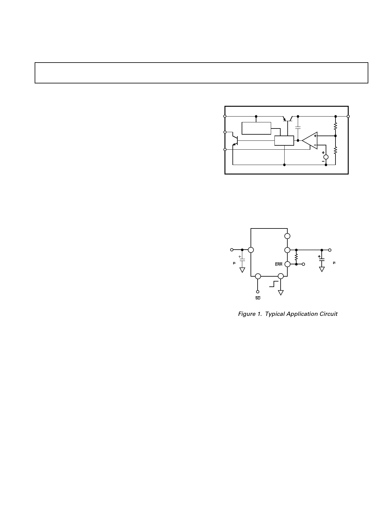
FUNCTIONAL BLOCK DIAGRAM
IN
ERR
Q2
SD
Q1
THERMAL
PROTECTION
DRIVER
GND
ADP3300
CC
Gm
BANDGAP
REF
OUT
R1
R2
VIN
C1
0.47 F
NR 2
ADP3300-5
5 IN
OUT 4
6
3
ON
OFF
1
GND
R1
330kΩ
EOUT
VOUT = +5V
C2
0.47 F
Figure 1. Typical Application Circuit
LDO family offers a wide range of output voltages and output
current levels from 50 mA to 200 mA:
ADP3301 (100 mA)
ADP3302 (100 mA, Dual Output)
ADP3303 (200 mA)
anyCAP is a registered trademark of Analog Devices Inc.
REV. A
Information furnished by Analog Devices is believed to be accurate and
reliable. However, no responsibility is assumed by Analog Devices for its
use, nor for any infringements of patents or other rights of third parties
which may result from its use. No license is granted by implication or
otherwise under any patent or patent rights of Analog Devices.
One Technology Way, P.O. Box 9106, Norwood, MA 02062-9106, U.S.A.
Tel: 781/329-4700 World Wide Web Site: http://www.analog.com
Fax: 781/326-8703
© Analog Devices, Inc., 2000
1 page 
3.220
3.210
VOUT = 3.2V
3.200
3.190
3.180
RL = 3.2kΩ
CL = 0.47µF
3.220
3.210
3.200
3.190
3.180
VOUT = 3.2V
RL = 64Ω
CL = 0.47µF
7.5
VIN
7.0
0 20 40 60 80 100 120 140 160 180 200
TIME – µs
Figure 11. Line Transient Response
7.5
7.0
0 20 40 60 80 100 120 140 160 180 200
TIME – µs
Figure 12. Line Transient Response
3.220
3.205
VOUT = 3.2V
CL = 4.7µF
3.200
3.195
3.190
IOUT = 50mA
50
1mA
1
0 200 400 600 800 1000
TIME – µs
Figure 14. Load Transient
3.0 VOUT = 3.0V
0
VOUT
200
150
100 IOUT
50
VIN = 7V
0
012 345
TIME – sec
Figure 15. Short Circuit Current
ADP3300
3.220
3.205
3.200
VOUT = 3.2V
CL = 0.47µF
3.195
3.190
50 IOUT = 50mA
1mA
1
0 200 400 600 800 1000
TIME – µs
Figure 13. Load Transient
4
CL = 0.47µF
3
2
1
0
+3
0
VOUT
3.2V
CL = 4.7µF
VOUT = 3.2V
RL = 64Ω
V
+3V
0 20 40 60 80 100
TIME – s
Figure 16. Turn On
4
3.2V
3
2
1
0
VOUT = 3.2V
RL = 64Ω
CL = 0.47µF
3V
0
0 20 40 60 80
TIME – µs
Figure 17. Turn Off
100
0
–10 a. 0.47µF, RL = 33kΩ
b. 0.47µF, RL = 64Ω
–20 c. 4.7µF, RL = 33kΩ
–30 d. 4.7µF, RL = 64Ω
–40
–50
–60
–70 b d
a
VOUT = 3.3V
b
d
c
–80
–90
ac
–100
10 100
1k
10k 100k 1M 10M
FREQUENCY – Hz
Figure 18. Power Supply Ripple
Rejection
10
0.47µF BYPASS
PIN 5 TO PIN 1
VOUT = 5V, CL = 0.47µF,
IL = 1mA, CNR = 0
1
VOUT = 3.3V, CL = 0.47µF,
IL = 1mA, CNR = 0
0.1 VOUT = 2.7-5.0V, CL = 0.47µF,
IL = 1mA, CNR = 10nF
VOUT = 2.7-5.0V, CL = 0.47µF,
IL = 1mA, CNR = 10nF
0.01
100
1k 10k
FREQUENCY – Hz
100k
Figure 19. Output Noise Density
REV. A
–5–
5 Page | ||
| Páginas | Total 8 Páginas | |
| PDF Descargar | [ Datasheet ADP3300.PDF ] | |
Hoja de datos destacado
| Número de pieza | Descripción | Fabricantes |
| ADP3300 | High Accuracy anyCAP 50 mA Low Dropout Linear Regulator | Analog Devices |
| ADP3301 | High Accuracy anyCAP 100 mA Low Dropout Linear Regulator | Analog Devices |
| ADP3302 | High Precision anyCAP Dual Low Dropout Linear Regulator | Analog Devices |
| ADP3302 | High Accuracy anyCAP 100 mA Low Dropout Linear Regulator | Analog Devices |
| Número de pieza | Descripción | Fabricantes |
| SLA6805M | High Voltage 3 phase Motor Driver IC. |
Sanken |
| SDC1742 | 12- and 14-Bit Hybrid Synchro / Resolver-to-Digital Converters. |
Analog Devices |
|
DataSheet.es es una pagina web que funciona como un repositorio de manuales o hoja de datos de muchos de los productos más populares, |
| DataSheet.es | 2020 | Privacy Policy | Contacto | Buscar |