|
|
|
PDF ADM697 Data sheet ( Hoja de datos )
| Número de pieza | ADM697 | |
| Descripción | Microprocessor Supervisory Circuits | |
| Fabricantes | Analog Devices | |
| Logotipo | ||
Hay una vista previa y un enlace de descarga de ADM697 (archivo pdf) en la parte inferior de esta página. Total 12 Páginas | ||
|
No Preview Available !
a
FEATURES
Superior Upgrade for MAX696/MAX697
Specified Over Temperature
Adjustable Low Line Voltage Monitor
Power OK/Reset Time Delay
Reset Assertion Down to 1 V VCC
Watchdog Timer—100 ms, 1.6 s, or Adjustable
Low Switch On Resistance
1.5 ⍀ Normal, 20 ⍀ in Backup
600 nA Standby Current
Automatic Battery Backup Switching (ADM696)
Fast On-Board Gating of Chip Enable Signals (ADM697)
Voltage Monitor for Power Fail or Low Battery Warning
APPLICATIONS
Microprocessor Systems
Computers
Controllers
Intelligent Instruments
Automotive Systems
Critical P Power Monitoring
GENERAL DESCRIPTION
The ADM696/ADM697 supervisory circuits offer complete
single chip solutions for power supply monitoring and battery
control functions in microprocessor systems. These functions
include µP reset, backup-battery switchover, watchdog timer,
CMOS RAM write protection, and power failure warning.
The ADM696/ADM697 are available in 16-pin DIP and small
outline packages and provide the following functions:
1. Power-On Reset output during power-up, power-down and
brownout conditions. The RESET voltage threshold is
adjustable using an external voltage divider. The RESET
output remains operational with VCC as low as 1 V.
2. A Reset pulse if the optional watchdog timer has not been
toggled within specified time.
3. Separate watchdog time-out and low line status outputs.
4. Adjustable reset and watchdog timeout periods.
5. A 1.3 V threshold detector for power fail warning, low bat-
tery detection, or to monitor a power supply other than VCC.
6. Battery backup switching for CMOS RAM, CMOS micro-
processor or other low power logic (ADM696).
7. Write protection of CMOS RAM or EEPROM (ADM697).
Microprocessor
Supervisory Circuits
ADM696/ADM697
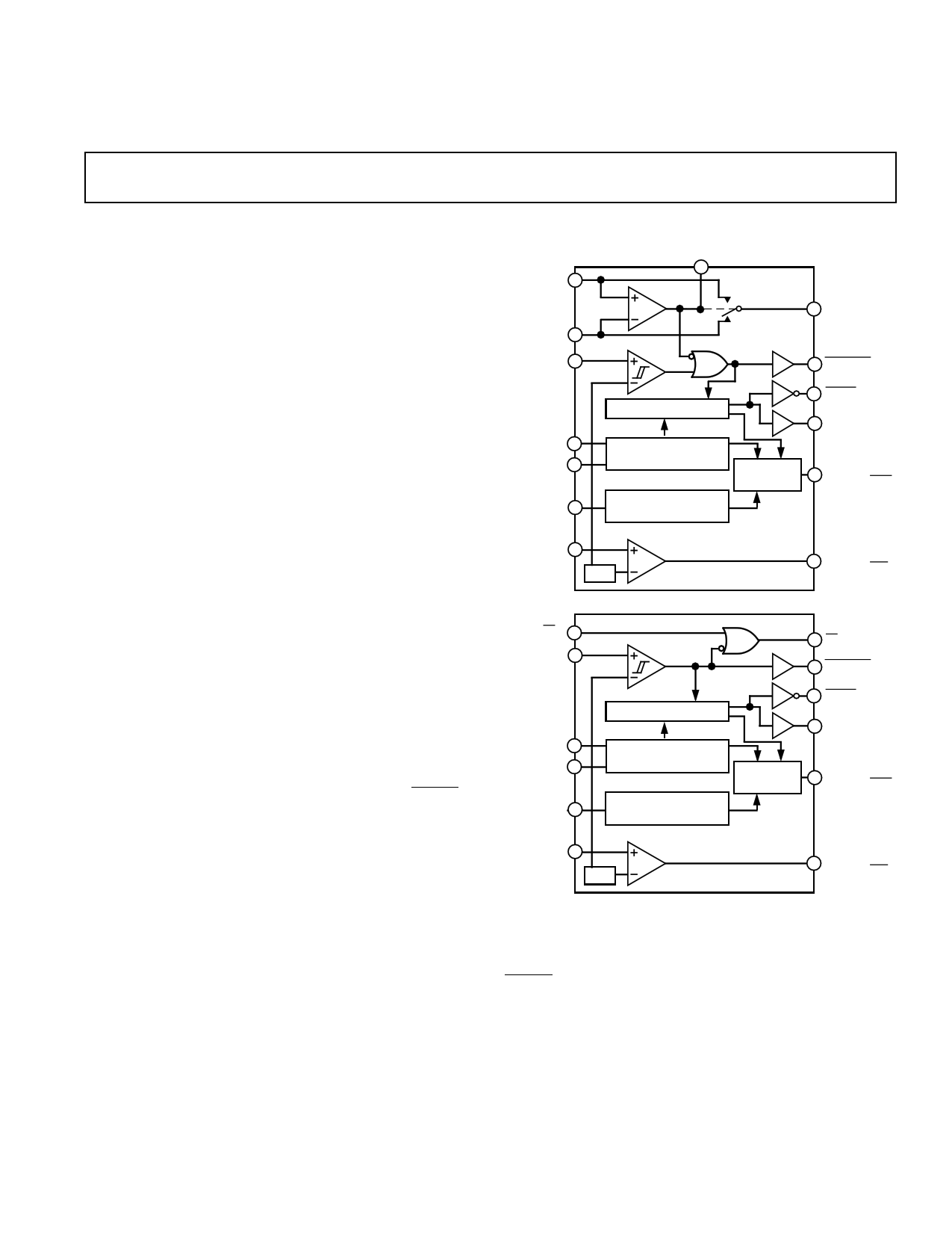
FUNCTIONAL BLOCK DIAGRAMS
VBATT
BATT ON
VCC
LLIN
OSC IN
OSC SEL
WATCHDOG
INPUT (WDI)
POWER FAIL
INPUT (PFI)
RESET GENERATOR
TIMEBASE FOR RESET
AND WATCHDOG
WATCHDOG
TRANSITION DETECTOR
WATCHDOG
TIMER
ADM696
1.3V
VOUT
LOW LINE
RESET
RESET
WATCHDOG
OUTPUT (WDO)
POWER FAIL
OUTPUT (PFO)
CEIN
LLIN
OSC IN
OSC SEL
WATCHDOG
INPUT (WDI)
POWER FAIL
INPUT (PFI)
RESET GENERATOR
TIMEBASE FOR RESET
AND WATCHDOG
WATCHDOG
TRANSITION DETECTOR
WATCHDOG
TIMER
ADM697
1.3V
CEOUT
LOW LINE
RESET
RESET
WATCHDOG
OUTPUT (WDO)
POWER FAIL
OUTPUT (PFO)
The ADM696/ADM697 is fabricated using an advanced epitaxial
CMOS process combining low power consumption (5 mW),
extremely fast Chip Enable gating (5 ns) and high reliability.
RESET assertion is guaranteed with VCC as low as 1 V. In
addition, the power switching circuitry is designed for minimal
voltage drop thereby permitting increased output current drive
of up to 100 mA without the need for an external pass transistor.
REV. 0
Information furnished by Analog Devices is believed to be accurate and
reliable. However, no responsibility is assumed by Analog Devices for its
use, nor for any infringements of patents or other rights of third parties
which may result from its use. No license is granted by implication or
otherwise under any patent or patent rights of Analog Devices.
One Technology Way, P.O. Box 9106, Norwood, MA 02062-9106, U.S.A.
Tel: 617/329-4700
Fax: 617/326-8703
1 page 
CIRCUIT INFORMATION
Battery-Switchover Section (ADM696)
The battery switchover circuit compares VCC to the VBATT
input, and connects VOUT to whichever is higher. Switchover
occurs when VCC is 50 mV higher than VBATT as VCC falls, and
when VCC is 70 mV greater than VBATT as VCC rises. This
20 mV of hysteresis prevents repeated rapid switching if VCC
falls very slowly or remains nearly equal to the battery voltage.
During normal operation with VCC higher than VBATT, VCC is
internally switched to VOUT via an internal PMOS transistor
switch. This switch has a typical on resistance of 1.5 Ω and can
supply up to 100 mA at the VOUT terminal. VOUT is normally
used to drive a RAM memory bank which may require instanta-
neous currents of greater than 100 mA. If this is the case, then
a bypass capacitor should be connected to VOUT. The capacitor
will provide the peak current transients to the RAM. A capaci-
tance value of 0.1 µF or greater may be used.
If the continuous output current requirement at VOUT exceeds
100 mA or if a lower VCC–VOUT voltage differential is desired,
an external PNP pass transistor may be connected in parallel
with the internal transistor. The BATT ON output can directly
drive the base of the external transistor.
A 20 Ω MOSFET switch connects the VBATT input to VOUT
during battery backup. This MOSFET has very low input-to-
output differential (dropout voltage) at the low current levels
required for battery backup of CMOS RAM or other low power
CMOS circuitry. The supply current in battery backup is typi-
cally 0.6 µA.
The ADM696 operates with battery voltages from 2.0 V to VCC
–0.3 V). High value capacitors, either standard electrolytic or
the farad-size double layer capacitors, can also be used for short-
term memory backup. A small charging current of typically
10 nA (0.1 µA max) flows out of the VBATT terminal. This cur-
rent is useful for maintaining rechargeable batteries in a fully
charged condition. This extends the life of the backup battery
by compensating for its self discharge current. Also note that
this current poses no problem when lithium batteries are used
for backup since the maximum charging current (0.1 µA) is safe
for even the smallest lithium cells.
If the battery-switchover section is not used, VBATT should be
connected to GND and VOUT should be connected to VCC.
VCC
VBATT
VOUT
GATE DRIVE
100
mV
700
mV
INTERNAL
SHUT DOWN SIGNAL
WHEN
VBATT > (VCC + 0.7V)
BATT ON
(ADM691, ADM693,
ADM695, ADM696)
Figure 1. Battery Switchover Schematic
ADM696/ADM697
Low Line RESET OUTPUT
RESET is an active low output which provides a RESET signal
to the microprocessor whenever the Low Line Input (LLIN) is
below 1.3 V. The LLIN input is normally used to monitor the
power supply voltage. An internal timer holds RESET low for
50 ms after the voltage on LLIN rises above 1.3 V. This is in-
tended as a power-on RESET signal for the processor. It allows
time for the power supply and microprocessor to stabilize. On
power-down, the RESET output remains low with VCC as low
as 1 V. This ensures that the microprocessor is held in a stable
shutdown condition.
The LLIN comparator has approximately 12 mV of hysteresis
for enhanced noise immunity.
In addition to RESET, an active high RESET output is also
available. This is the complement of RESET and is useful for
processors requiring an active high RESET.
LL
IN
RESET
V2
t1
V1
V2
t1
V1
LOW LINE
t1 = RESET TIME
V1 = RESET VOLTAGE THRESHOLD LOW
V2 = RESET VOLTAGE THRESHOLD HIGH
HYSTERESIS = V2–V1
Figure 2. Power-Fail Reset Timing
Watchdog Timer RESET
The watchdog timer circuit monitors the activity of the micro-
processor in order to check that it is not stalled in an indefinite
loop. An output line on the processor is used to toggle the
Watchdog Input (WDI) line. If this line is not toggled within
the selected timeout period, a RESET pulse is generated. The
ADM696/ADM697 may be configured for either a fixed
“short” 100 ms or a “long” 1.6 second timeout period or for an
adjustable timeout period. If the “short” period is selected some
systems may be unable to service the watchdog timer immedi-
ately after a reset, so a “long” timeout is automatically initiated
directly after a reset is issued. The watchdog timer is restarted
at the end of Reset, whether the Reset was caused by lack of ac-
tivity on WDI or by LLIN falling below the reset threshold.
The normal (short) timeout period becomes effective following
the first transition of WDI after RESET has gone inactive. The
watchdog timeout period restarts with each transition on the
WDI pin. To ensure that the watchdog timer does not time out,
either a high-to-low or low-to high transition on the WDI pin
must occur at or less than the minimum timeout period. If WDI
remains permanently either high or low, reset pulses will be is-
sued after each timeout period (1.6 s). The watchdog monitor
can be deactivated by floating the Watchdog Input (WDI) or by
connecting it to midsupply.
REV. 0
–5–
5 Page 
This application also shows an optional, external transistor
which may be used to provide in excess of 100 mA current on
VOUT. When VCC is higher than VBATT, the BATT ON output
goes low, providing 25 mA of base drive for the external PNP
transistor. The maximum current available is dependent on the
power rating of the external transistor.
ADM696/ADM697
RAM Write Protection
The ADM697 CEOUT line drives the Chip Select inputs of the
CMOS RAM. CEOUT follows CEIN as long as LLIN is above the
reset threshold. If LLIN falls below the reset threshold, CEOUT
goes high, independent of the logic level at CEIN. This prevents
the microprocessor from writing erroneous data into RAM dur-
ing power-up, power-down, brownouts and momentary power
interruptions.
OUTLINE DIMENSIONS
Dimensions shown in inches and (mm).
16-Pin Plastic DIP (N-16)
PIN 1
1
6
1
9
0.280 (7.11)
0.240 (6.10)
8
0.210
(5.33)
0.200 (5.05)
0.125 (3.18)
0.840 (21.33)
0.745 (18.93)
0.060 (1.52)
0.015 (0.38)
0.150
(3.81)
0.022 (0.558) 0.100 (2.54)
0.014 (0.356)
BSC
0.070 (1.77)
0.045 (1.15)
SEATING
PLANE
0.325 (8.25)
0.300 (7.62)
0.195 (4.95)
0.115 (2.93)
0.015 (0.381)
0.008 (0.204)
16-Pin Cerdip (Q-16)
16
PIN 1
1
9
0.310 (7.87)
0.220 (5.59)
8
0.200
(5.08)
MAX
SEATING
PLANE
0.840 (21.34) MAX
0.060 (1.52)
0.015 (0.38)
0.150
(3.81)
MIN
0.022 (0.558)
0.014 (0.356)
0.100 (2.54)
BSC
0.070 (1.78)
0.30 (0.76)
0.320 (8.13)
0.290 (7.37)
0.015 (0.381)
0.008 (0.204)
16-Lead SOIC (R-16)
16
0.299
(7.60)
9
0.419
(10.65)
18
0.012
(0.3)
0.413 (10.50)
0.030
(0.75)
0.104
(2.65)
0.05 (1.27) 0.019 (0.49)
REF
0.013
(0.32)
0.042
(1.07)
REV. 0
–11–
11 Page | ||
| Páginas | Total 12 Páginas | |
| PDF Descargar | [ Datasheet ADM697.PDF ] | |
Hoja de datos destacado
| Número de pieza | Descripción | Fabricantes |
| ADM690 | Microprocessor Supervisory Circuits | Analog Devices |
| ADM690A | Microprocessor Supervisory Circuits | Analog Devices |
| ADM691 | Microprocessor Supervisory Circuits | Analog Devices |
| ADM691A | Microprocessor Supervisory Circuits | Analog Devices |
| Número de pieza | Descripción | Fabricantes |
| SLA6805M | High Voltage 3 phase Motor Driver IC. |
Sanken |
| SDC1742 | 12- and 14-Bit Hybrid Synchro / Resolver-to-Digital Converters. |
Analog Devices |
|
DataSheet.es es una pagina web que funciona como un repositorio de manuales o hoja de datos de muchos de los productos más populares, |
| DataSheet.es | 2020 | Privacy Policy | Contacto | Buscar |