|
|
|
PDF ADM694 Data sheet ( Hoja de datos )
| Número de pieza | ADM694 | |
| Descripción | Microprocessor Supervisory Circuits | |
| Fabricantes | Analog Devices | |
| Logotipo | ||
Hay una vista previa y un enlace de descarga de ADM694 (archivo pdf) en la parte inferior de esta página. Total 16 Páginas | ||
|
No Preview Available !
a
Microprocessor
Supervisory Circuits
ADM690–ADM695
FEATURES
Superior Upgrade for MAX690–MAX695
Specified Over Temperature
Low Power Consumption (5 mW)
Precision Voltage Monitor
Reset Assertion Down to 1 V VCC
Low Switch On-Resistance 1.5 ⍀ Normal,
20 ⍀ in Backup
High Current Drive (100 mA)
Watchdog Timer—100 ms, 1.6 s, or Adjustable
600 nA Standby Current
Automatic Battery Backup Power Switching
Extremely Fast Gating of Chip Enable Signals (5 ns)
Voltage Monitor for Power Fail
APPLICATIONS
Microprocessor Systems
Computers
Controllers
Intelligent Instruments
Automotive Systems
GENERAL DESCRIPTION
The ADM690–ADM695 family of supervisory circuits offers
complete single chip solutions for power supply monitoring and
battery control functions in microprocessor systems. These
functions include µP reset, backup battery switchover, watchdog
timer, CMOS RAM write protection, and power failure warn-
ing. The complete family provides a variety of configurations to
satisfy most microprocessor system requirements.
The ADM690, ADM692 and ADM694 are available in 8-pin
DIP packages and provide:
1. Power-on reset output during power-up, power-down and
brownout conditions. The RESET output remains opera-
tional with VCC as low as 1 V.
2. Battery backup switching for CMOS RAM, CMOS
microprocessor or other low power logic.
3. A reset pulse if the optional watchdog timer has not been
toggled within a specified time.
4. A 1.3 V threshold detector for power fail warning, low battery
detection, or to monitor a power supply other than +5 V.
The ADM691, ADM693 and ADM695 are available in 16-pin
DIP and small outline packages and provide three additional
functions.
1. Write protection of CMOS RAM or EEPROM.
2. Adjustable reset and watchdog timeout periods.
3. Separate watchdog timeout, backup battery switchover, and
low VCC status outputs.
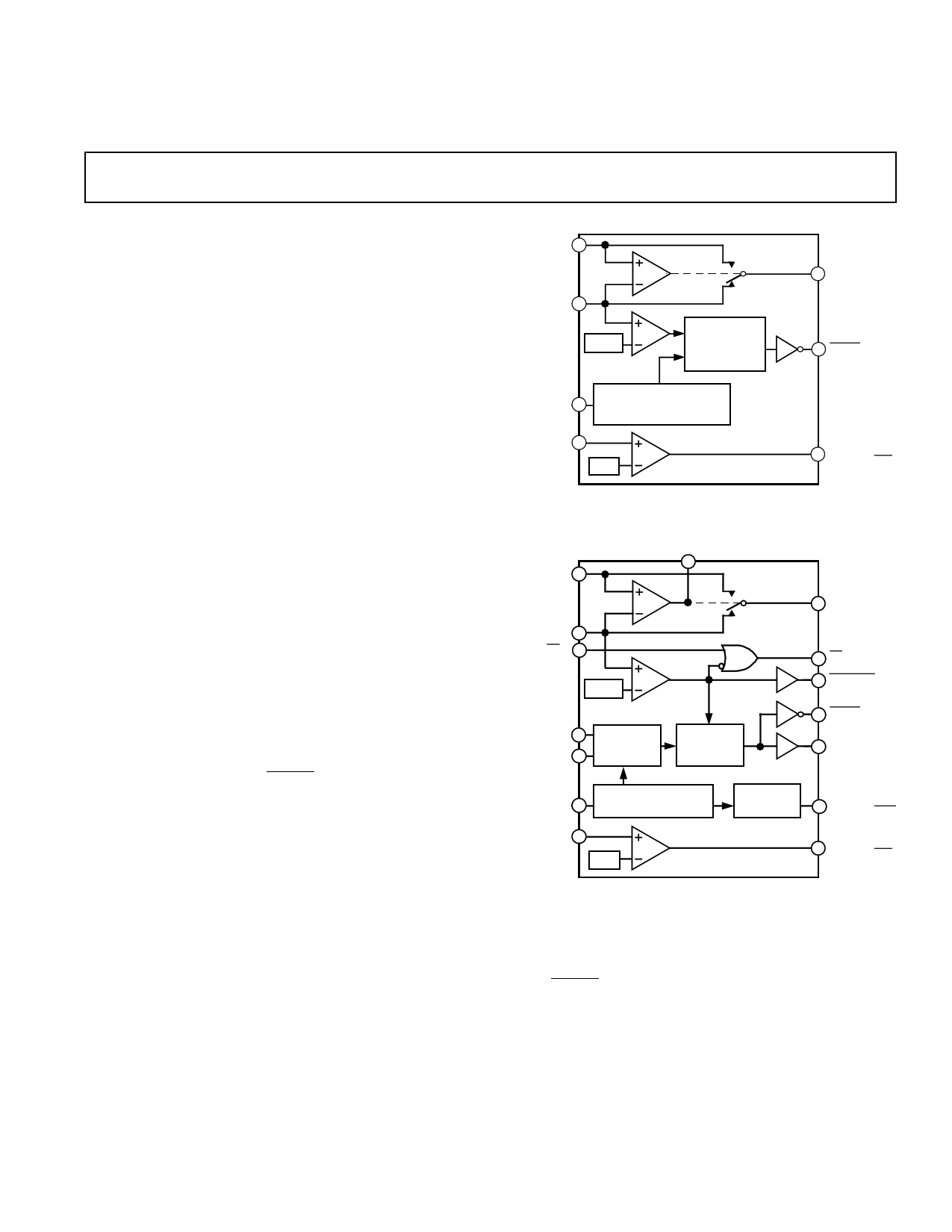
FUNCTIONAL BLOCK DIAGRAMS
VBATT
VOUT
VCC
4.65V 1
RESET
GENERATOR2
RESET
WATCHDOG
INPUT (WDI)
POWER FAIL
INPUT (PFI)
WATCHDOG
TRANSITION DETECTOR
(1.6s)
1.3V
ADM690
ADM692
ADM694
POWER FAIL
OUTPUT (PFO)
1VOLTAGE DETECTOR = 4.65V (ADM690, ADM694)
4.40V (ADM692)
2RESET PULSE WIDTH = 50ms (ADM690, ADM692)
200ms (ADM694)
BATT ON
VBATT
VCC
CEIN
4.65V 1
OSC IN
OSC SEL
RESET &
WATCHDOG
TIMEBASE
ADM691
ADM693
ADM695
VOUT
CEOUT
LOW LINE
RESET
GENERATOR
RESET
RESET
WATCHDOG
INPUT (WDI)
POWER FAIL
INPUT (PFI)
WATCHDOG
TRANSITION DETECTOR
1.3V
WATCHDOG
TIMER
WATCHDOG
OUTPUT (WDO)
POWER FAIL
OUTPUT (PFO)
1VOLTAGE DETECTOR = 4.65V (ADM691, ADM695)
4.40V (ADM693)
The ADM690–ADM695 family is fabricated using an advanced
epitaxial CMOS process combining low power consumption
(5 mW), extremely fast Chip Enable gating (5 ns) and high reli-
ability. RESET assertion is guaranteed with VCC as low as 1 V.
In addition, the power switching circuitry is designed for mini-
mal voltage drop thereby permitting increased output current
drive of up to 100 mA without the need for an external pass
transistor.
REV. A
Information furnished by Analog Devices is believed to be accurate and
reliable. However, no responsibility is assumed by Analog Devices for its
use, nor for any infringements of patents or other rights of third parties
which may result from its use. No license is granted by implication or
otherwise under any patent or patent rights of Analog Devices.
© Analog Devices, Inc., 1996
One Technology Way, P.O. Box 9106, Norwood, MA 02062-9106, U.S.A.
Tel: 617/329-4700
Fax: 617/326-8703
1 page 
ADM690–ADM695
PIN CONFIGURATIONS
VBATT 1
VOUT 2
VCC 3
GND 4
BATT ON 5
LOW LINE 6
ADM691
ADM693
ADM695
TOP VIEW
(Not to Scale)
16 RESET
15 RESET
14 WDO
13 CEIN
12 CEOUT
11 WDI
OSC IN 7
10 PFO
OSC SEL 8
9 PFI
VOUT 1
VCC 2
GND 3
PFI 4
ADM690
ADM692
ADM694
TOP VIEW
(Not to Scale)
8 VBATT
7 RESET
6 WDI
5 PFO
Part
Number
ADM690
ADM691
ADM692
ADM693
ADM694
ADM695
Nominal Reset
Time
50 ms
50 ms or ADJ
50 ms
50 ms or ADJ
200 ms
200 ms or ADJ
PRODUCT SELECTION GUIDE
Nominal VCC
Reset Threshold
Nominal Watchdog Battery Backup
Timeout Period
Switching
4.65 V
4.65 V
4.4 V
4.4 V
4.65 V
4.65 V
1.6 s
100 ms, 1.6 s, ADJ
1.6 s
100 ms, 1.6 s, ADJ
1.6 s
100 ms, 1.6 s, ADJ
Yes
Yes
Yes
Yes
Yes
Yes
Base Drive
Ext PNP
No
Yes
No
Yes
No
Yes
Chip Enable
Signals
No
Yes
No
Yes
No
Yes
CIRCUIT INFORMATION
Battery Switchover Section
The battery switchover circuit compares VCC to the VBATT
input, and connects VOUT to whichever is higher. Switchover
occurs when VCC is 50 mV higher than VBATT as VCC falls, and
when VCC is 70 mV greater than VBATT as VCC rises. This
20 mV of hysteresis prevents repeated rapid switching if VCC
falls very slowly or remains nearly equal to the battery voltage.
Figure 1. Battery Switchover Schematic
During normal operation with VCC higher than VBATT, VCC is in-
ternally switched to VOUT via an internal PMOS transistor
switch. This switch has a typical on-resistance of 1.5 Ω and can
supply up to 100 mA at the VOUT terminal. VOUT is normally
used to drive a RAM memory bank which may require instanta-
neous currents of greater than 100 mA. If this is the case then a
bypass capacitor should be connected to VOUT. The capacitor
will provide the peak current transients to the RAM. A capaci-
tance value of 0.1 µF or greater may be used.
If the continuous output current requirement at VOUT exceeds
100 mA or if a lower VCC–VOUT voltage differential is desired,
an external PNP pass transistor may be connected in parallel
with the internal transistor. The BATT ON output (ADM691/
ADM693/ADM695) can directly drive the base of the external
transistor.
A 20 Ω MOSFET switch connects the VBATT input to VOUT
during battery backup. This MOSFET has very low input-to-
output differential (dropout voltage) at the low current levels
required for battery back up of CMOS RAM or other low
power CMOS circuitry. The supply current in battery back up
is typically 0.6 µA.
The ADM690/ADM691/ADM694/ADM695 operates with
battery voltages from 2.0 V to 4.25 V and the ADM692/ADM693
operates with battery voltages from 2.0 V to 4.0 V. High value
capacitors, either standard electrolytic or the farad size double
layer capacitors, can also be used for short-term memory back
up. A small charging current of typically 10 nA (0.1 µA max)
flows out of the VBATT terminal. This current is useful for
maintaining rechargeable batteries in a fully charged condition.
This extends the life of the back up battery by compensating
for its self discharge current. Also note that this current poses
no problem when lithium batteries are used for back up since
the maximum charging current (0.1 µA) is safe for even the
smallest lithium cells.
If the battery-switchover section is not used, VBATT should be
connected to GND and VOUT should be connected to VCC.
REV. A
–5–
5 Page 
ADM690–ADM695
BATTERY
20kΩ
OPTIONAL
TEST LOAD
+5V INPUT
POWER
VBATT
10MΩ
PFI
VCC
ADM69x
PFO
LOW BATTERY
SIGNAL TO
µP I/O PIN
10MΩ
CEOUT
CEIN
FROM µP I/O PIN
APPLIES TEST LOAD
TO BATTERY
CONTROL
INPUT*
D1
OSC SEL
D2 ADM69x
OSC IN
*LOW = INTERNAL TIMEOUT
HIGH = EXTERNAL TIMEOUT
Figure 20. Monitoring the Battery Status
Alternate Watchdog Input Drive Circuits
The watchdog feature can be enabled and disabled under pro-
gram control by driving WDI with a 3-state buffer (Figure 21a).
When three-stated, the WDI input will float thereby disabling
the watchdog timer.
WATCHDOG
STROBE
CONTROL
INPUT
WDI
ADM69x
Figure 21a. Programming the Watchdog Input
This circuit is not entirely foolproof, and it is possible that a
software fault could erroneously 3-state the buffer. This would
then prevent the ADM69x from detecting that the microproces-
sor is no longer operating correctly. In most cases a better
method is to extend the watchdog period rather than disabling
the watchdog. This may be done under program control using
the circuit shown in Figure 21b. When the control input is high,
the OSC SEL pin is low and the watchdog timeout is set by the
external capacitor. A 0.01 µF capacitor sets a watchdog timeout
delay of 100 seconds. When the control input is low, the OSC
SEL pin is driven high, selecting the internal oscillator. The
100 ms or the 1.6 s period is chosen, depending on which diode
in Figure 21b is used. With D1 inserted the internal timeout is
set at 100 ms, while with D2 inserted the timeout is set at 1.6 s.
Figure 21b. Programming the Watchdog Input
Replacing the Backup Battery
When changing the backup battery with system power on, spuri-
ous resets can occur when the battery is removed. This occurs
because the leakage current flowing out of the VBATT pin will
charge up the stray capacitance. If the voltage on VBATT reaches
within 50 mV of VCC, a reset pulse is generated.
If spurious resets during battery replacement are acceptable,
then no action is required. If not, then one of the following
solutions should be considered:
1. A capacitor from VBATT to GND. This gives time while the
capacitor is charging up to replace the battery. The leakage
current will charge up the external capacitor towards the VCC
level. The time taken is related to the charging current, the
size of external capacitor and the voltage differential between
the capacitor and the charging voltage supply.
t = CEXT × VDIFF/I
The maximum leakage (charging) current is 1 µA over tem-
perature and VDIFF = VCC–VBATT. Therefore, the capacitor
size should be chosen such that sufficient time is available to
make the battery replacement.
CEXT = TREQD (1 µA/(VCC–VBATT))
If a replacement time of 5 seconds is allowed and assuming a
VCC of 4.5 V and a VBATT of 3 V
CEXT = 3.33 µF
BATTERY
VBATT
CEXT
ADM69x
Figure 22a. Preventing Spurious RESETS During
Battery Replacement
2. A resistor from VBATT to GND. This will prevent the voltage
on VBATT from rising to within 50 mV of VCC during battery
replacement.
REV. A
–11–
11 Page | ||
| Páginas | Total 16 Páginas | |
| PDF Descargar | [ Datasheet ADM694.PDF ] | |
Hoja de datos destacado
| Número de pieza | Descripción | Fabricantes |
| ADM690 | Microprocessor Supervisory Circuits | Analog Devices |
| ADM690A | Microprocessor Supervisory Circuits | Analog Devices |
| ADM691 | Microprocessor Supervisory Circuits | Analog Devices |
| ADM691A | Microprocessor Supervisory Circuits | Analog Devices |
| Número de pieza | Descripción | Fabricantes |
| SLA6805M | High Voltage 3 phase Motor Driver IC. |
Sanken |
| SDC1742 | 12- and 14-Bit Hybrid Synchro / Resolver-to-Digital Converters. |
Analog Devices |
|
DataSheet.es es una pagina web que funciona como un repositorio de manuales o hoja de datos de muchos de los productos más populares, |
| DataSheet.es | 2020 | Privacy Policy | Contacto | Buscar |