|
|
|
PDF ADG836 Data sheet ( Hoja de datos )
| Número de pieza | ADG836 | |
| Descripción | 0.5CMOS 1.65 V TO 3.6 V Dual SPDT/2:1 MUX | |
| Fabricantes | Analog Devices | |
| Logotipo | ||
Hay una vista previa y un enlace de descarga de ADG836 (archivo pdf) en la parte inferior de esta página. Total 12 Páginas | ||
|
No Preview Available !
FEATURES
0.5 Typical On Resistance
0.8 Maximum On Resistance at 125°C
1.65 V to 3.6 V Operation
Automotive Temperature Range: –40°C to +125°C
High Current Carrying Capability: 300 mA Continuous
Rail-to-Rail Switching Operation
Fast Switching Times <20 ns
Typical Power Consumption (<0.1 W)
APPLICATIONS
Cellular Phones
PDAs
MP3 Players
Power Routing
Battery-Powered Systems
PCMCIA Cards
Modems
Audio and Video Signal Routing
Communication Systems
0.5 CMOS 1.65 V TO 3.6 V
Dual SPDT/2:1 MUX
ADG836
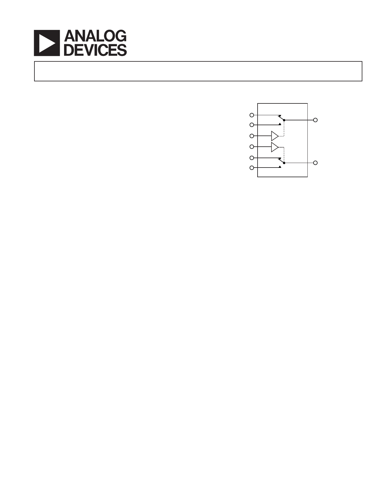
FUNCTIONAL BLOCK DIAGRAM
������
���
���
���
���
���
���
��
��
�������� ����� ��� � ����� � �����
GENERAL DESCRIPTION
The ADG836 is a low voltage CMOS device containing two
independently selectable single-pole, double-throw (SPDT)
switches. This device offers ultralow on resistance of less than
0.8 over the full temperature range. The ADG836 is fully
specified for 3.3 V, 2.5 V, and 1.8 V supply operation.
Each switch conducts equally well in both directions when on
and has an input signal range that extends to the supplies. The
ADG836 exhibits break-before-make switching action.
The ADG836 is available in 10-lead MSOP and 3 mm 3 mm
12-lead LFCSP packages.
PRODUCT HIGHLIGHTS
1. <0.8 over full temperature range of –40°C to +125°C.
2. Single 1.65 V to 3.6 V operation.
3. Compatible with 1.8 V CMOS logic.
4. High current handling capability (300 mA continuous current
at 3.3 V).
5. Low THD + N (0.02% typ).
6. 3 mm 3 mm LFCSP package and 10-lead MSOP package.
REV. 0
Information furnished by Analog Devices is believed to be accurate and
reliable. However, no responsibility is assumed by Analog Devices for its
use, nor for any infringements of patents or other rights of third parties
that may result from its use. No license is granted by implication or oth-
erwise under any patent or patent rights of Analog Devices.Trademarks
and registered trademarks are the property of their respective companies.
One Technology Way, P.O. Box 9106, Norwood, MA 02062-9106, U.S.A.
Tel: 781/329-4700
www.analog.com
Fax: 781/326-8703
© 2003 Analog Devices, Inc. All rights reserved.
1 page 
ABSOLUTE MAXIMUM RATINGS1
(TA = 25°C, unless otherwise noted.)
VDD to GND . . . . . . . . . . . . . . . . . . . . . . . . . . –0.3 V to +4.6 V
Analog Inputs2 . . . . . . . . . . . . . . . . . . . . . –0.3 V to VDD + 0.3 V
Digital Inputs2 . . . . . . . . . . . . . . . . . . . . . . . . . . –0.3 V to 4.6 V
or 10 mA, Whichever Occurs First
Peak Current, S or D
3.3 V Operation . . . . . . . . . . . . . . . . . . . . . . . . . . . . . 500 mA
2.5 V Operation . . . . . . . . . . . . . . . . . . . . . . . . . . . . . 460 mA
1.8 V Operation . . . . . . . . . . . . . . . . . . . . . . . . . . . . . 420 mA
(Pulsed at 1ms, 10% Duty Cycle Max)
Continuous Current, S or D
3.3 V Operation
300 mA
2.5 V Operation
275 mA
1.8 V Operation
250 mA
Operating Temperature Range
Automotive (Y Version) . . . . . . . . . . . . . . . . –40°C to +125°C
Storage Temperature Range . . . . . . . . . . . . . . –65°C to +150°C
Junction Temperature . . . . . . . . . . . . . . . . . . . . . . . . . . . .150°C
MSOP Package
JA Thermal Impedance . . . . . . . . . . . . . . . . . . . . . . 206°C/W
JC Thermal Impedance . . . . . . . . . . . . . . . . . . . . . . . 44°C/W
LFCSP Package
JA Thermal Impedance (3-Layer Board) . . . . . . . . . 61.1°C/W
IR Reflow, Peak Temperature <20 sec . . . . . . . . . . . . . . . .235°C
NOTES
1 Stresses above those listed under Absolute Maximum Ratings may cause permanent
damage to the device.This is a stress rating only; functional operation of the device
at these or any other conditions above those listed in the operational sections of this
specification is not implied. Exposure to absolute maximum rating conditions for
extended periods may affect device reliability. Only one absolute maximum rating
may be applied at any one time.
2 Overvoltages at IN, S, or D will be clamped by internal diodes. Current should be
limited to the maximum ratings given.
Logic
0
1
ADG836
Table I. ADG836 Truth Table
Switch A
Switch B
Off On
On Off
ORDERING GUIDE
Model
Temperature Range Package Description
ADG836YRM
ADG836YRM-REEL
ADG836YRM-REEL7
ADG836YCP
ADG836YCP-REEL
ADG836YCP-REEL7
–40°C to +125°C
–40°C to +125°C
–40°C to +125°C
–40°C to +125°C
–40°C to +125°C
–40°C to +125°C
Mini Small Outline Package (MSOP)
Mini Small Outline Package (MSOP)
Mini Small Outline Package (MSOP)
Lead Frame Chip Scale Package (LFCSP)
Lead Frame Chip Scale Package (LFCSP)
Lead Frame Chip Scale Package (LFCSP)
*Branding on this package is limited to three characters due to space constraints.
Package Option
RM-10
RM-10
RM-10
CP-12
CP-12
CP-12
Branding*
S9A
S9A
S9A
S9A
S9A
S9A
CAUTION
ESD (electrostatic discharge) sensitive device. Electrostatic charges as high as 4000V readily accumulate
on the human body and test equipment and can discharge without detection. Although the ADG836
features proprietary ESD protection circuitry, permanent damage may occur on devices subjected to high
energy electrostatic discharges.Therefore, proper ESD precautions are recommended to avoid performance
degradation or loss of functionality.
REV. 0
–5–
5 Page 
���
�����
���
��
��� ���
���
�
���
�������
��������
���
��
�� ����
���
��� ��������� � �� ���
����
��
Test Circuit 7. Off Isolation
���
�����
���
���
���
�
���
�������
��������
���
��
�� ����
���
��������� ���� � �� ���
���� ���� ������
���� ������� ������
Test Circuit 8. Bandwidth
�������
��������
����
��
���
���
��
ADG836
���
�����
���
���
���
� ��
���
���
������������������ ��������� � �� ���
����
��
Test Circuit 9. Channel-to-Channel Crosstalk (S1A–S1B)
�������
��������
����
���
���
��
���
���
��
���
���
��
��
�� ���
������������������ ��������� � �� ���
����
��
Test Circuit 10. Channel-to-Channel Crosstalk (S1A–S2A)
REV. 0
–11–
11 Page | ||
| Páginas | Total 12 Páginas | |
| PDF Descargar | [ Datasheet ADG836.PDF ] | |
Hoja de datos destacado
| Número de pieza | Descripción | Fabricantes |
| ADG836 | 0.5CMOS 1.65 V TO 3.6 V Dual SPDT/2:1 MUX | Analog Devices |
| ADG836L | 0.5 OHM CMOS 1.65 V to 3.6 V Dual SPDT/2:1 MUX | Analog Devices |
| ADG839 | Single SPDT Switch/2:1 MUX | Analog Devices |
| Número de pieza | Descripción | Fabricantes |
| SLA6805M | High Voltage 3 phase Motor Driver IC. |
Sanken |
| SDC1742 | 12- and 14-Bit Hybrid Synchro / Resolver-to-Digital Converters. |
Analog Devices |
|
DataSheet.es es una pagina web que funciona como un repositorio de manuales o hoja de datos de muchos de los productos más populares, |
| DataSheet.es | 2020 | Privacy Policy | Contacto | Buscar |