|
|
|
PDF ADSP-BF533 Data sheet ( Hoja de datos )
| Número de pieza | ADSP-BF533 | |
| Descripción | Blackfin Embedded Processor | |
| Fabricantes | Analog Devices | |
| Logotipo | ||
Hay una vista previa y un enlace de descarga de ADSP-BF533 (archivo pdf) en la parte inferior de esta página. Total 30 Páginas | ||
|
No Preview Available !
Blackfin
Embedded Processor
ADSP-BF531/ADSP-BF532/ADSP-BF533
FEATURES
Up to 600 MHz high performance Blackfin processor
Two 16-bit MACs, two 40-bit ALUs, four 8-bit video ALUs,
40-bit shifter
RISC-like register and instruction model for ease of pro-
gramming and compiler-friendly support
Advanced debug, trace, and performance monitoring
Wide range of operating voltages (see Operating Conditions
on Page 20)
Qualified for Automotive Applications (see Automotive Prod-
ucts on Page 62)
Programmable on-chip voltage regulator
160-ball CSP_BGA, 169-ball PBGA, and 176-lead LQFP
packages
MEMORY
Up to 148K bytes of on-chip memory (see Table 1 on Page 3)
Memory management unit providing memory protection
External memory controller with glueless support for
SDRAM, SRAM, flash, and ROM
Flexible memory booting options from SPI and
external memory
PERIPHERALS
Parallel peripheral interface PPI, supporting
ITU-R 656 video data formats
2 dual-channel, full duplex synchronous serial ports, sup-
porting eight stereo I2S channels
2 memory-to-memory DMAs
8 peripheral DMAs
SPI-compatible port
Three 32-bit timer/counters with PWM support
Real-time clock and watchdog timer
32-bit core timer
Up to 16 general-purpose I/O pins (GPIO)
UART with support for IrDA
Event handler
Debug/JTAG interface
On-chip PLL capable of frequency multiplication
VOLTAGE REGULATOR
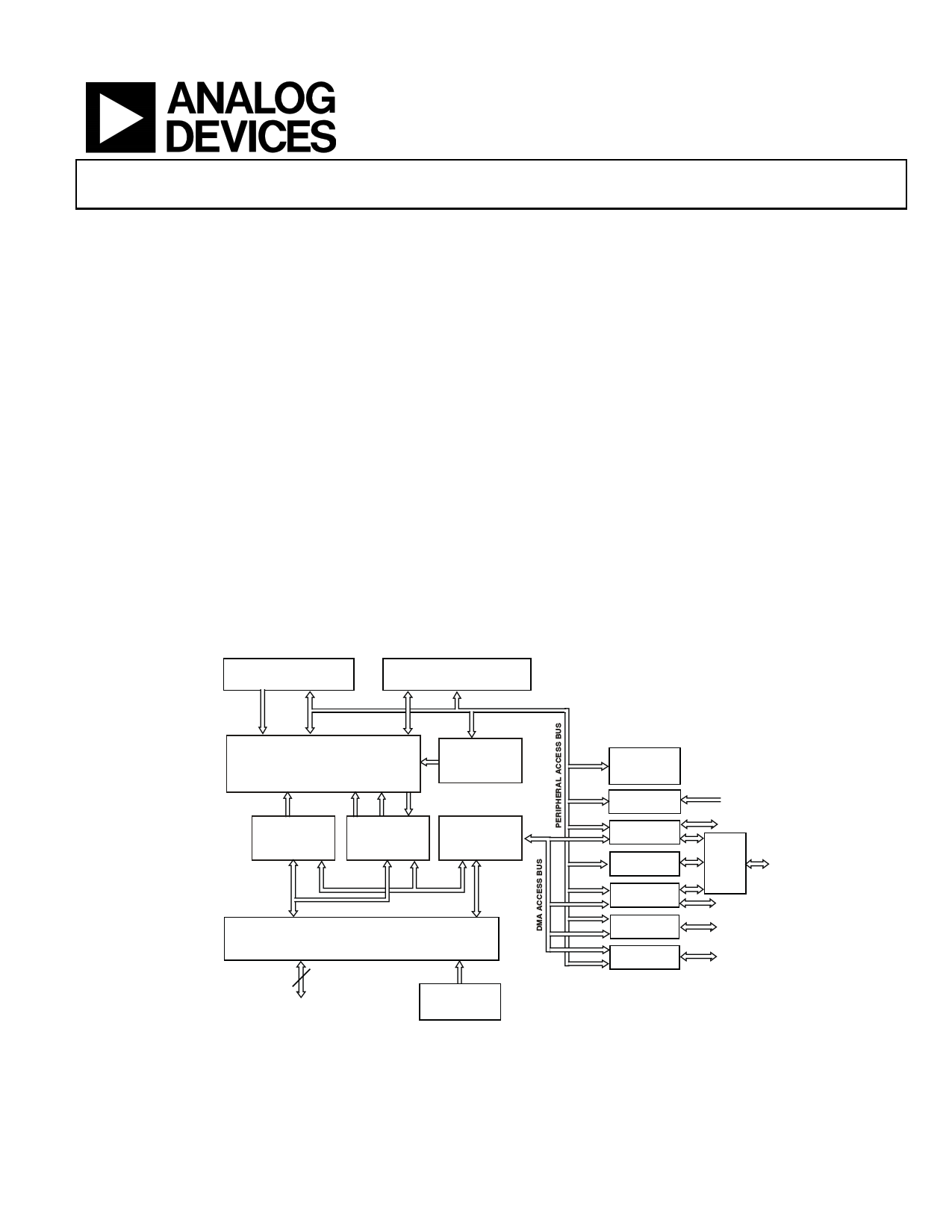
JTAG TEST AND EMULATION
B
INTERRUPT
CONTROLLER
L1
INSTRUCTION
MEMORY
L1
DATA
MEMORY
DMA
CONTROLLER
DMA CORE BUS
EXTERNAL ACCESS BUS
EXTERNAL PORT
FLASH, SDRAM CONTROL
DMA
EXTERNAL
BUS
16
BOOT ROM
WATCHDOG
TIMER
RTC
PPI
TIMER0-2
SPI
UART
SPORT0-1
GPIO
PORT
F
Figure 1. Functional Block Diagram
Blackfin and the Blackfin logo are registered trademarks of Analog Devices, Inc.
Rev. I
Document Feedback
Information furnished by Analog Devices is believed to be accurate and reliable.
However, no responsibility is assumed by Analog Devices for its use, nor for any
infringements of patents or other rights of third parties that may result from its use.
Specifications subject to change without notice. No license is granted by implication
or otherwise under any patent or patent rights of Analog Devices. Trademarks and
registered trademarks are the property of their respective owners.
One Technology Way, P.O. Box 9106, Norwood, MA 02062-9106 U.S.A.
Tel: 781.329.4700
©2013 Analog Devices, Inc. All rights reserved.
Technical Support
www.analog.com
1 page 
ADSP-BF531/ADSP-BF532/ADSP-BF533
ADDRESS ARITHMETIC UNIT
DA1 32
DA0 32
I3 L3 B3
I2 L2 B2
I1 L1 B1
I0 L0 B0
M3
M2
M1
M0
DAG1
32
RAB
DAG0
SP
FP
P5
P4
P3
P2
P1
P0
32
PREG
SD 32
LD1 32
LD0 32
32
32
R7.H
R6.H
R5.H
R4.H
R3.H
R2.H
R1.H
R0.H
R7.L
R6.L
R5.L
R4.L
R3.L
R2.L
R1.L
R0.L
8
BARREL
SHIFTER
16
40
A0
88
40 40
32 32
DATA ARITHMETIC UNIT
ASTAT
16
8
40
A1
SEQUENCER
ALIGN
DECODE
LOOP BUFFER
CONTROL
UNIT
Figure 2. Blackfin Processor Core
The second on-chip memory block is the L1 data memory, con-
sisting of one or two banks of up to 32K bytes. The memory
banks are configurable, offering both cache and SRAM func-
tionality. This memory block is accessed at full processor speed.
The third memory block is a 4K byte scratchpad SRAM, which
runs at the same speed as the L1 memories, but is only accessible
as data SRAM and cannot be configured as cache memory.
External (Off-Chip) Memory
External memory is accessed via the external bus interface unit
(EBIU). This 16-bit interface provides a glueless connection to a
bank of synchronous DRAM (SDRAM) as well as up to four
banks of asynchronous memory devices including flash,
EPROM, ROM, SRAM, and memory mapped I/O devices.
The PC133-compliant SDRAM controller can be programmed
to interface to up to 128M bytes of SDRAM. The SDRAM con-
troller allows one row to be open for each internal SDRAM
bank, for up to four internal SDRAM banks, improving overall
system performance.
The asynchronous memory controller can be programmed to
control up to four banks of devices with very flexible timing
parameters for a wide variety of devices. Each bank occupies a
1M byte segment regardless of the size of the devices used, so
that these banks are only contiguous if each is fully populated
with 1M byte of memory.
I/O Memory Space
Blackfin processors do not define a separate I/O space. All
resources are mapped through the flat 32-bit address space.
On-chip I/O devices have their control registers mapped into
memory mapped registers (MMRs) at addresses near the top of
the 4G byte address space. These are separated into two smaller
blocks, one containing the control MMRs for all core functions,
and the other containing the registers needed for setup and con-
trol of the on-chip peripherals outside of the core. The MMRs
are accessible only in supervisor mode and appear as reserved
space to on-chip peripherals.
Booting
The ADSP-BF531/ADSP-BF532/ADSP-BF533 processors con-
tain a small boot kernel, which configures the appropriate
peripheral for booting. If the processors are configured to boot
from boot ROM memory space, the processor starts executing
from the on-chip boot ROM. For more information, see Boot-
ing Modes on Page 14.
Rev. I | Page 5 of 64 | August 2013
5 Page 
ADSP-BF531/ADSP-BF532/ADSP-BF533
PFx pins defined as inputs can be configured to generate
hardware interrupts, while output PFx pins can be trig-
gered by software interrupts.
• GPIO interrupt sensitivity registers – The two GPIO inter-
rupt sensitivity registers specify whether individual PFx
pins are level- or edge-sensitive and specify—if edge-sensi-
tive—whether just the rising edge or both the rising and
falling edges of the signal are significant. One register
selects the type of sensitivity, and one register selects which
edges are significant for edge-sensitivity.
PARALLEL PERIPHERAL INTERFACE
The processors provide a parallel peripheral interface (PPI) that
can connect directly to parallel ADCs and DACs, video encod-
ers and decoders, and other general-purpose peripherals. The
PPI consists of a dedicated input clock pin, up to three frame
synchronization pins, and up to 16 data pins. The input clock
supports parallel data rates up to half the system clock rate and
the synchronization signals can be configured as either inputs or
outputs.
The PPI supports a variety of general-purpose and ITU-R 656
modes of operation. In general-purpose mode, the PPI provides
half-duplex, bi-directional data transfer with up to 16 bits of
data. Up to three frame synchronization signals are also pro-
vided. In ITU-R 656 mode, the PPI provides half-duplex bi-
directional transfer of 8- or 10-bit video data. Additionally, on-
chip decode of embedded start-of-line (SOL) and start-of-field
(SOF) preamble packets is supported.
General-Purpose Mode Descriptions
The general-purpose modes of the PPI are intended to suit a
wide variety of data capture and transmission applications.
Three distinct sub modes are supported:
• Input mode – Frame syncs and data are inputs into the PPI.
• Frame capture mode – Frame syncs are outputs from the
PPI, but data are inputs.
• Output mode – Frame syncs and data are outputs from the
PPI.
Input Mode
Input mode is intended for ADC applications, as well as video
communication with hardware signaling. In its simplest form,
PPI_FS1 is an external frame sync input that controls when to
read data. The PPI_DELAY MMR allows for a delay (in PPI_-
CLK cycles) between reception of this frame sync and the
initiation of data reads. The number of input data samples is
user programmable and defined by the contents of the
PPI_COUNT register. The PPI supports 8-bit and 10-bit
through 16-bit data, programmable in the PPI_CONTROL
register.
Frame Capture Mode
Frame capture mode allows the video source(s) to act as a slave
(e.g., for frame capture). The processors control when to read
from the video source(s). PPI_FS1 is an HSYNC output and
PPI_FS2 is a VSYNC output.
Output Mode
Output mode is used for transmitting video or other data with
up to three output frame syncs. Typically, a single frame sync is
appropriate for data converter applications, whereas two or
three frame syncs could be used for sending video with hard-
ware signaling.
ITU-R 656 Mode Descriptions
The ITU-R 656 modes of the PPI are intended to suit a wide
variety of video capture, processing, and transmission applica-
tions. Three distinct sub modes are supported:
• Active video only mode
• Vertical blanking only mode
• Entire field mode
Active Video Only Mode
Active video only mode is used when only the active video por-
tion of a field is of interest and not any of the blanking intervals.
The PPI does not read in any data between the end of active
video (EAV) and start of active video (SAV) preamble symbols,
or any data present during the vertical blanking intervals. In this
mode, the control byte sequences are not stored to memory;
they are filtered by the PPI. After synchronizing to the start of
Field 1, the PPI ignores incoming samples until it sees an SAV
code. The user specifies the number of active video lines per
frame (in PPI_COUNT register).
Vertical Blanking Interval Mode
In this mode, the PPI only transfers vertical blanking interval
(VBI) data.
Entire Field Mode
In this mode, the entire incoming bit stream is read in through
the PPI. This includes active video, control preamble sequences,
and ancillary data that can be embedded in horizontal and verti-
cal blanking intervals. Data transfer starts immediately after
synchronization to Field 1. Data is transferred to or from the
synchronous channels through eight DMA engines that work
autonomously from the processor core.
DYNAMIC POWER MANAGEMENT
The ADSP-BF531/ADSP-BF532/ADSP-BF533 processors pro-
vides four operating modes, each with a different performance/
power profile. In addition, dynamic power management pro-
vides the control functions to dynamically alter the processor
core supply voltage, further reducing power dissipation. Control
of clocking to each of the processor peripherals also reduces
power consumption. See Table 4 for a summary of the power
settings for each mode.
Full-On Operating Mode—Maximum Performance
In the full-on mode, the PLL is enabled and is not bypassed,
providing capability for maximum operational frequency. This
is the power-up default execution state in which maximum per-
formance can be achieved. The processor core and all enabled
peripherals run at full speed.
Rev. I | Page 11 of 64 | August 2013
11 Page | ||
| Páginas | Total 30 Páginas | |
| PDF Descargar | [ Datasheet ADSP-BF533.PDF ] | |
Hoja de datos destacado
| Número de pieza | Descripción | Fabricantes |
| ADSP-BF531 | Blackfin Embedded Processor | Analog Devices |
| ADSP-BF531SBBC400 | Blackfin Embedded Processor | Analog Devices |
| ADSP-BF531SBBZ400 | Blackfin Embedded Processor | Analog Devices |
| ADSP-BF531SBST400 | Blackfin Embedded Processor | Analog Devices |
| Número de pieza | Descripción | Fabricantes |
| SLA6805M | High Voltage 3 phase Motor Driver IC. |
Sanken |
| SDC1742 | 12- and 14-Bit Hybrid Synchro / Resolver-to-Digital Converters. |
Analog Devices |
|
DataSheet.es es una pagina web que funciona como un repositorio de manuales o hoja de datos de muchos de los productos más populares, |
| DataSheet.es | 2020 | Privacy Policy | Contacto | Buscar |