|
|
|
PDF ADSP-2185LBST-210 Data sheet ( Hoja de datos )
| Número de pieza | ADSP-2185LBST-210 | |
| Descripción | DSP Microcomputer | |
| Fabricantes | Analog Devices | |
| Logotipo | ||
Hay una vista previa y un enlace de descarga de ADSP-2185LBST-210 (archivo pdf) en la parte inferior de esta página. Total 31 Páginas | ||
|
No Preview Available !
a
DSP Microcomputer
ADSP-2185L
FEATURES
PERFORMANCE
19 ns Instruction Cycle Time @ 3.3 Volts, 52 MIPS
Sustained Performance
Single-Cycle Instruction Execution
Single-Cycle Context Switch
3-Bus Architecture Allows Dual Operand Fetches in
Every Instruction Cycle
Multifunction Instructions
Power-Down Mode Featuring Low CMOS Standby
Power Dissipation with 400 Cycle Recovery from
Power-Down Condition
Low Power Dissipation in Idle Mode
INTEGRATION
ADSP-2100 Family Code Compatible, with Instruction
Set Extensions
80K Bytes of On-Chip RAM, Configured as 16K Words
Program Memory RAM and 16K Words
Data Memory RAM
Dual Purpose Program Memory for Instruction␣ and Data
Storage
Independent ALU, Multiplier/Accumulator and Barrel
Shifter Computational Units
Two Independent Data Address Generators
Powerful Program Sequencer Provides Zero Overhead
Looping Conditional Instruction Execution
Programmable 16-Bit Interval Timer with Prescaler
100-Lead LQFP
SYSTEM INTERFACE
16-Bit Internal DMA Port for High Speed Access to
On-Chip Memory (Mode Selectable)
4 MByte Memory Interface for Storage of Data Tables
and Program Overlays (Mode Selectable)
8-Bit DMA to Byte Memory for Transparent Program
and Data Memory Transfers (Mode Selectable)
I/O Memory Interface with 2048 Locations Supports
Parallel Peripherals (Mode Selectable)
Programmable Memory Strobe and Separate I/O Memory
Space Permits “Glueless” System Design
Programmable Wait State Generation
Two Double-Buffered Serial Ports with Companding
Hardware and Automatic Data Buffering
Automatic Booting of On-Chip Program Memory from
Byte-Wide External Memory, e.g., EPROM, or
Through Internal DMA Port
Six External Interrupts
13 Programmable Flag Pins Provide Flexible System
Signaling
UART Emulation through Software SPORT Reconfiguration
ICE-Port™ Emulator Interface Supports Debugging in
Final Systems
ICE-Port is a trademark of Analog Devices, Inc.
REV. A
Information furnished by Analog Devices is believed to be accurate and
reliable. However, no responsibility is assumed by Analog Devices for its
use, nor for any infringements of patents or other rights of third parties
which may result from its use. No license is granted by implication or
otherwise under any patent or patent rights of Analog Devices.
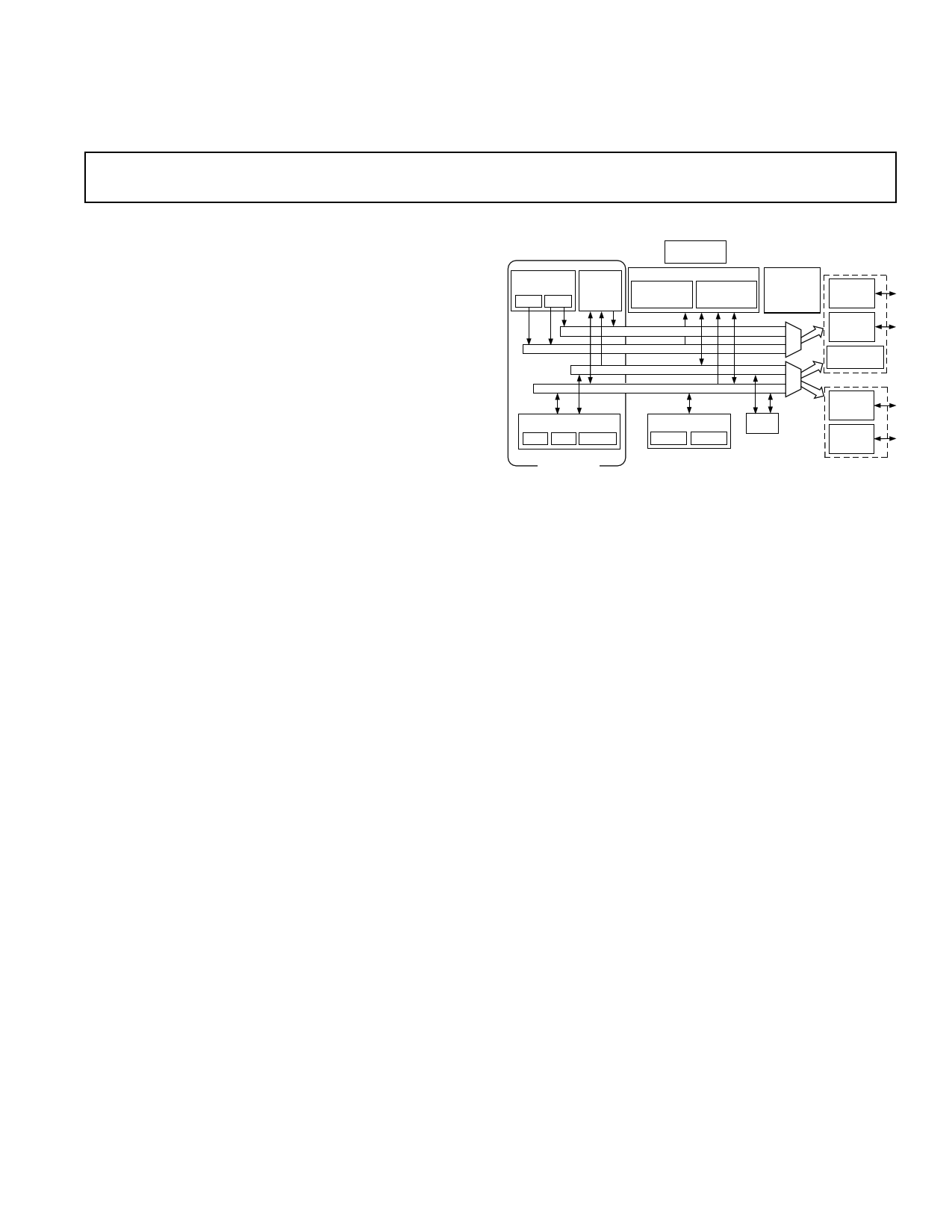
FUNCTIONAL BLOCK DIAGRAM
DATA ADDRESS
GENERATORS
DAG 1 DAG 2
PROGRAM
SEQUENCER
POWER-DOWN
CONTROL
MEMORY
16K؋24 PM
16K؋16 DM
( ) ( )8K؋24 OVERLAY 1
8K؋24 OVERLAY 2
8K؋16 OVERLAY 1
8K؋16 OVERLAY 2
PROGRAMMABLE
I/O
AND
FLAGS
FULL MEMORY
MODE
EXTERNAL
ADDRESS
BUS
PROGRAM MEMORY ADDRESS
DATA MEMORY ADDRESS
PROGRAM MEMORY DATA
DATA MEMORY DATA
ARITHMETIC UNITS
ALU MAC SHIFTER
ADSP-2100 BASE
ARCHITECTURE
SERIAL PORTS
SPORT 0 SPORT 1
TIMER
EXTERNAL
DATA
BUS
BYTE DMA
CONTROLLER
OR
EXTERNAL
DATA
BUS
INTERNAL
DMA
PORT
HOST MODE
GENERAL NOTE
This data sheet represents specifications for the ADSP-2185L
3.3 V processor.
GENERAL DESCRIPTION
The ADSP-2185L is a single-chip microcomputer optimized for
digital signal processing (DSP) and other high speed numeric
processing applications.
The ADSP-2185L combines the ADSP-2100 family base archi-
tecture (three computational units, data address generators and
a program sequencer) with two serial ports, a 16-bit internal
DMA port, a byte DMA port, a programmable timer, Flag I/O,
extensive interrupt capabilities and on-chip program and data
memory.
The ADSP-2185L integrates 80K bytes of on-chip memory
configured as 16K words (24-bit) of program RAM, and 16K
words (16-bit) of data RAM. Power-down circuitry is also pro-
vided to meet the low power needs of battery operated portable
equipment. The ADSP-2185L is available in 100-lead LQFP
package.
In addition, the ADSP-2185L supports instructions which
include bit manipulations—bit set, bit clear, bit toggle, bit test—
ALU constants, multiplication instruction (x squared), biased
rounding, result free ALU operations, I/O memory transfers and
global interrupt masking, for increased flexibility.
Fabricated in a high speed, low power, CMOS process, the
ADSP-2185L operates with a 19 ns instruction cycle time. Ev-
ery instruction can execute in a single processor cycle.
␣␣
One Technology Way, P.O. Box 9106, Norwood, MA 02062-9106, U.S.A.
Tel: 781/329-4700
World Wide Web Site: http://www.analog.com
Fax: 781/326-8703
© Analog Devices, Inc., 1998
1 page 
Pin Terminations (Continued)
Pin
Name
I/O
3-State
(Z)
Reset
State
Hi-Z*
Caused
By
Unused
Configuration
D4 or
IS
D3 or
IACK
D2:0 or
IAD15:13
PMS
DMS
BMS
IOMS
CMS
RD
WR
BR
BG
BGH
IRQ2/PF7
I/O (Z)
I
I/O (Z)
I/O (Z)
I/O (Z)
O (Z)
O (Z)
O (Z)
O (Z)
O (Z)
O (Z)
O (Z)
I
O (Z)
O
I/O (Z)
Hi-Z
I
Hi-Z
Hi-Z
Hi-Z
O
O
O
O
O
O
O
I
O
O
I
IRQL1/PF6 I/O (Z) I
IRQL0/PF5 I/O (Z) I
IRQE/PF4 I/O (Z) I
SCLK0
I/O
RFS0
DR0
TFS0
DT0
SCLK1
I/O
I
I/O
O
I/O
RFS1/RQ0
DR1/FI
TFS1/RQ1
DT1/FO
EE
EBR
EBG
ERESET
EMS
EINT
ECLK
ELIN
ELOUT
I/O
I
I/O
O
I
I
O
I
O
I
I
I
O
I
I
I
O
O
I
I
I
O
O
I
I
O
I
O
I
I
I
O
BR, EBR
BR, EBR
BR, EBR
IS
BR, EBR
BR, EBR
BR, EBR
BR, EBR
BR, EBR
BR, EBR
BR, EBR
EE
Float
High (Inactive)
Float
Float
Float
Float
Float
Float
Float
Float
Float
Float
Float
High (Inactive)
Float
Float
Input = High (Inactive)
or Program as Output,
Set to 1, Let Float
Input = High (Inactive)
or Program as Output,
Set to 1, Let Float
Input = High (Inactive)
or Program as Output,
Set to 1, Let Float
Input = High (Inactive)
or Program as Output,
Set to 1, Let Float
Input = High or Low,
Output = Float
High or Low
High or Low
High or Low
Float
Input = High or Low,
Output = Float
High or Low
High or Low
High or Low
Float
NOTES
**Hi-Z = High Impedance.
1. If the CLKOUT pin is not used, turn it OFF.
2. If the Interrupt/Programmable Flag pins are not used, there are two options:
Option 1: When these pins are configured as INPUTS at reset and function as
interrupts and input flag pins, pull the pins High (inactive).
Option 2: Program the unused pins as OUTPUTS, set them to 1, and let
them float.
3. All bidirectional pins have three-stated outputs. When the pins is configured
as an output, the output is Hi-Z (high impedance) when inactive.
4. CLKIN, RESET, and PF3:0 are not included in the table because these pins
must be used.
ADSP-2185L
Interrupts
The interrupt controller allows the processor to respond to the
eleven possible interrupts and reset with minimum overhead.
The ADSP-2185L provides four dedicated external interrupt
input pins, IRQ2, IRQL0, IRQL1 and IRQE. In addition,
SPORT1 may be reconfigured for IRQ0, IRQ1, FLAG_IN and
FLAG_OUT, for a total of six external interrupts. The ADSP-
2185L also supports internal interrupts from the timer, the byte
DMA port, the two serial ports, software and the power-down
control circuit. The interrupt levels are internally prioritized and
individually maskable (except power down and reset). The
IRQ2, IRQ0 and IRQ1 input pins can be programmed to be
either level- or edge-sensitive. IRQL0 and IRQL1 are level-
sensitive and IRQE is edge sensitive. The priorities and vector
addresses of all interrupts are shown in Table I.
Table I. Interrupt Priority and Interrupt Vector Addresses
Source of Interrupt
Interrupt Vector
Address (Hex)
RESET (or Power-Up with PUCR = 1)
Power-Down (Nonmaskable)
IRQ2
IRQL1
IRQL0
SPORT0 Transmit
SPORT0 Receive
IRQE
BDMA Interrupt
SPORT1 Transmit or IRQ1
SPORT1 Receive or IRQ0
Timer
0000 (Highest Priority)
002C
0004
0008
000C
0010
0014
0018
001C
0020
0024
0028 (Lowest Priority)
Interrupt routines can either be nested with higher priority inter-
rupts taking precedence or processed sequentially. Interrupts
can be masked or unmasked with the IMASK register. Indi-
vidual interrupt requests are logically ANDed with the bits in
IMASK; the highest priority unmasked interrupt is then se-
lected. The power-down interrupt is nonmaskable.
The ADSP-2185L masks all interrupts for one instruction cycle
following the execution of an instruction that modifies the
IMASK register. This does not affect serial port auto-
buffering or DMA transfers.
The interrupt control register, ICNTL, controls interrupt nest-
ing and defines the IRQ0, IRQ1 and IRQ2 external interrupts to
be either edge- or level-sensitive. The IRQE pin is an external
edge-sensitive interrupt and can be forced and cleared. The
IRQL0 and IRQL1 pins are external level-sensitive interrupts.
The IFC register is a write-only register used to force and clear
interrupts. On-chip stacks preserve the processor status and are
automatically maintained during interrupt handling. The stacks are
twelve levels deep to allow interrupt, loop and subroutine nest-
ing. The following instructions allow global enable or disable
servicing of the interrupts (including power down), regardless of
the state of IMASK. Disabling the interrupts does not affect se-
rial port autobuffering or DMA.
ENA INTS;
DIS INTS;
When the processor is reset, interrupt servicing is enabled.
REV. A
–5–
5 Page 
ADSP-2185L
IDMA CONTROL (U = UNDEFINED AT RESET)
15 14 13 12 11 10 9 8 7 6 5 4 3 2 1 0
U U U U U U U U U U U U U U U DM(0؋3FE0)
IDMAA
ADDRESS
IDMAD
DESTINATION MEMORY TYPE:
0 = PM
1 = DM
Figure 8. IDMA Control/OVLAY Registers
Bootstrap Loading (Booting)
The ADSP-2185L has two mechanisms to allow automatic
loading of the internal program memory after reset. The method
for booting after reset is controlled by the Mode A, B and C
configuration bits.
When the mode pins specify BDMA booting, the ADSP-2185L
initiates a BDMA boot sequence when reset is released.
The BDMA interface is set up during reset to the following de-
faults when BDMA booting is specified: the BDIR, BMPAGE,
BIAD and BEAD registers are set to 0, the BTYPE register is
set to 0 to specify program memory 24-bit words, and the
BWCOUNT register is set to 32. This causes 32 words of on-
chip program memory to be loaded from byte memory. These
32 words are used to set up the BDMA to load in the remaining
program code. The BCR bit is also set to 1, which causes pro-
gram execution to be held off until all 32 words are loaded into
on-chip program memory. Execution then begins at address 0.
The ADSP-2100 Family Development Software (Revision 5.02
and later) fully supports the BDMA booting feature and can
generate byte memory space compatible boot code.
The IDLE instruction can also be used to allow the processor to
hold off execution while booting continues through the BDMA
interface. For BDMA accesses while in Host Mode, the ad-
dresses to boot memory must be constructed externally to the
ADSP-2185L. The only memory address bit provided by the
processor is A0.
IDMA Port Booting
The ADSP-2185L can also boot programs through its Internal
DMA port. If Mode C = 1, Mode B = 0 and Mode A = 1, the
ADSP-2185L boots from the IDMA port. IDMA feature can
load as much on-chip memory as desired. Program execution is
held off until on-chip program memory location 0 is written to.
Bus Request and Bus Grant (Full Memory Mode)
The ADSP-2185L can relinquish control of the data and ad-
dress buses to an external device. When the external device re-
quires access to memory, it asserts the bus request (BR) signal.
If the ADSP-2185L is not performing an external memory ac-
cess, it responds to the active BR input in the following proces-
sor cycle by:
• three-stating the data and address buses and the PMS, DMS,
BMS, CMS, IOMS, RD, WR output drivers,
• asserting the bus grant (BG) signal, and
• halting program execution.
If Go Mode is enabled, the ADSP-2185L will not halt program
execution until it encounters an instruction that requires an ex-
ternal memory access.
If the ADSP-2185L is performing an external memory access
when the external device asserts the BR signal, it will not three-
state the memory interfaces or assert the BG signal until the
processor cycle after the access completes. The instruction does
not need to be completed when the bus is granted. If a single in-
struction requires two external memory accesses, the bus will be
granted between the two accesses.
When the BR signal is released, the processor releases the BG
signal, reenables the output drivers and continues program ex-
ecution from the point at which it stopped.
The bus request feature operates at all times, including when
the processor is booting and when RESET is active.
The BGH pin is asserted when the ADSP-2185L is ready to ex-
ecute an instruction, but is stopped because the external bus is
already granted to another device. The other device can release
the bus by deasserting bus request. Once the bus is released, the
ADSP-2185L deasserts BG and BGH and executes the external
memory access.
Flag I/O Pins
The ADSP-2185L has eight general purpose programmable
input/output flag pins. They are controlled by two memory
mapped registers. The PFTYPE register determines the direc-
tion, 1 = output and 0 = input. The PFDATA register is used to
read and write the values on the pins. Data being read from a
pin configured as an input is synchronized to the ADSP-2185L’s
clock. Bits that are programmed as outputs will read the value
being output. The PF pins default to input during reset.
In addition to the programmable flags, the ADSP-2185L has
five fixed-mode flags, FLAG_IN, FLAG_OUT, FL0, FL1 and
FL2. FL0-FL2 are dedicated output flags. FLAG_IN and
FLAG_OUT are available as an alternate configuration of
SPORT1.
Note: Pins PF0, PF1, PF2 and PF3 are also used for device
configuration during reset.
INSTRUCTION SET DESCRIPTION
The ADSP-2185L assembly language instruction set has an
algebraic syntax that was designed for ease of coding and read-
ability. The assembly language, which takes full advantage of
the processor’s unique architecture, offers the following benefits:
• The algebraic syntax eliminates the need to remember cryptic
assembler mnemonics. For example, a typical arithmetic add
instruction, such as AR = AX0 + AY0, resembles a simple
equation.
• Every instruction assembles into a single, 24-bit word that can
execute in a single instruction cycle.
• The syntax is a superset ADSP-2100 Family assembly lan-
guage and is completely source and object code compatible
with other family members. Programs may need to be relo-
cated to utilize on-chip memory and conform to the ADSP-
2185L’s interrupt vector and reset vector map.
• Sixteen condition codes are available. For conditional jump,
call, return or arithmetic instructions, the condition can be
checked and the operation executed in the same instruction
cycle.
• Multifunction instructions allow parallel execution of an
arithmetic instruction with up to two fetches or one write to
processor memory space during a single instruction cycle.
REV. A
–11–
11 Page | ||
| Páginas | Total 31 Páginas | |
| PDF Descargar | [ Datasheet ADSP-2185LBST-210.PDF ] | |
Hoja de datos destacado
| Número de pieza | Descripción | Fabricantes |
| ADSP-2185LBST-210 | DSP Microcomputer | Analog Devices |
| Número de pieza | Descripción | Fabricantes |
| SLA6805M | High Voltage 3 phase Motor Driver IC. |
Sanken |
| SDC1742 | 12- and 14-Bit Hybrid Synchro / Resolver-to-Digital Converters. |
Analog Devices |
|
DataSheet.es es una pagina web que funciona como un repositorio de manuales o hoja de datos de muchos de los productos más populares, |
| DataSheet.es | 2020 | Privacy Policy | Contacto | Buscar |