|
|
PDF ADS8321 Data sheet ( Hoja de datos )
| Número de pieza | ADS8321 | |
| Descripción | 16-Bit/ High Speed/ MicroPower Sampling ANALOG-TO-DIGITAL CONVERTER | |
| Fabricantes | Burr-Brown Corporation | |
| Logotipo |  |
|
Hay una vista previa y un enlace de descarga de ADS8321 (archivo pdf) en la parte inferior de esta página. Total 12 Páginas | ||
|
No Preview Available !
® ADS8321
For most current data sheet and other product
information, visit www.burr-brown.com
16-Bit, High Speed, MicroPower Sampling
ANALOG-TO-DIGITAL CONVERTER
FEATURES
q BIPOLAR INPUT RANGE
q 100kHz SAMPLING RATE
q MICRO POWER:
4.5mW at 100kHz
1mW at 10kHz
q POWER DOWN: 3µA max
q 8-LEAD MSOP PACKAGE
q PIN-COMPATIBLE TO ADS7816 AND
ADS7822
q SERIAL (SPI/SSI) INTERFACE
APPLICATIONS
q BATTERY OPERATED SYSTEMS
q REMOTE DATA ACQUISITION
q ISOLATED DATA ACQUISITION
q SIMULTANEOUS SAMPLING,
MULTI-CHANNEL SYSTEMS
q INDUSTRIAL CONTROLS
q ROBOTICS
q VIBRATION ANALYSIS
DESCRIPTION
The ADS8321 is a 16-bit sampling analog-to-digital
converter with guaranteed specifications over a 4.75V
to 5.25V supply range. It requires very little power
even when operating at the full 100kHz data rate. At
lower data rates, the high speed of the device enables
it to spend most of its time in the power-down mode—
the average power dissipation is less than 1mW at
10kHz data rate.
The ADS8321 also features a synchronous serial
(SPI/SSI compatible) interface, and a differential in-
put. The reference voltage can be set to any level
within the range of 500mV to 2.5V.
Ultra-low power and small size make the ADS8321
ideal for portable and battery-operated systems. It is
also a perfect fit for remote data acquisition mod-
ules, simultaneous multi-channel systems, and iso-
lated data acquisition. The ADS8321 is available in
an 8-lead MSOP package.
VREF
+In
–In
SAR
ADS8321
S/H Amp
CDAC
Comparator
Serial
Interface
DOUT
DCLOCK
CS/SHDN
International Airport Industrial Park • Mailing Address: PO Box 11400, Tucson, AZ 85734 • Street Address: 6730 S. Tucson Blvd., Tucson, AZ 85706 • Tel: (520) 746-1111
Twx: 910-952-1111 • Internet: http://www.burr-brown.com/ • Cable: BBRCORP • Telex: 066-6491 • FAX: (520) 889-1510 • Immediate Product Info: (800) 548-6132
©1999 Burr-Brown Corporation
PDS-1537A
Printed in U.S.A. Setpember, 1999
1 page 
TYPICAL PERFORMANCE CURVES (Cont.)
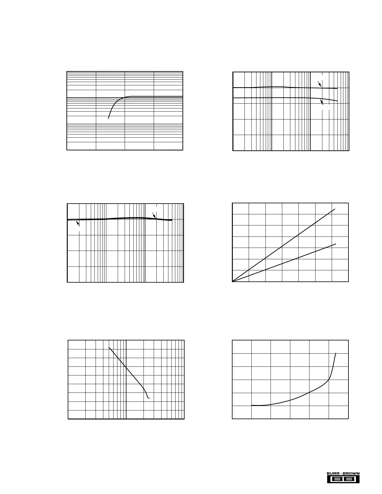
At TA = +25°C, VCC = +5V, VREF = +2.5V, fSAMPLE = 100kHz, fCLK = 24 • fSAMPLE, unless otherwise specified.
1000
MAXIMUM SAMPLE RATE vs VCC
100
10
1
12345
VCC (V)
SIGNAL-TO-NOISE AND SIGNAL-TO-(NOISE + DISTORTION)
vs INPUT FREQUENCY
90
SNR
85
80
SINAD
75
70
65
0.1
1 10
Input Frequency (kHz)
100
SPURIOUS FREE DYNAMIC RANGE AND
TOTAL HARMONIC DISTORTION vs INPUT FREQUENCY
90
SFDR
85
THD
80
75
70
65
0.1
1 10
Input Frequency (kHz)
100
35
30
25
20
15
10
5
0
0
REFERENCE CURRENT vs SAMPLE RATE
2.5V
1.25V
20 40 60 80 100 120 140
Sample Rate (kHz)
18
16
14
12
10
8
6
4
2
0
0.1
NOISE vs REFERENCE VOLTAGE
1
Reference Voltage (V)
10
15
10
5
0
–5
–10
–15
0
CHANGE IN GAIN vs REFERENCE VOLTAGE
0.5 1.0 1.5 2.0 2.5 3.0
Reference Voltage (V)
®
5 ADS8321
5 Page 
1000
100
TA = 25°C
VCC = 5.0V
VREF = 2.5V
fCLK = 2.4MHz
10
1
0.1
1 10
Sample Rate (kHz)
100
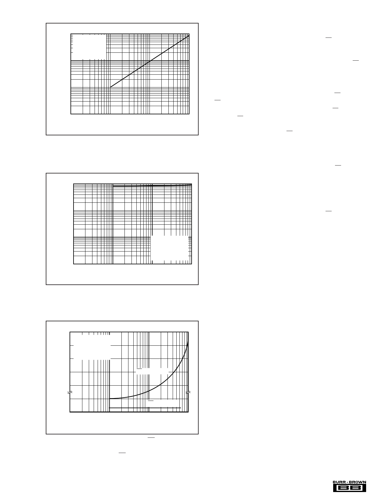
FIGURE 8. Maintaining fCLK at the Highest Possible Rate
Allows Supply Current to Drop Linearly with
Sample Rate.
1000
100
10
1
0.1
TA = 25°C
VCC = 5.0V
VREF = 2.5V
fCLK = 24 • fSAMPLE
1 10
Sample Rate (kHz)
100
FIGURE 9. Scaling fCLK Reduces Supply Current Only
Slightly with Sample Rate.
Figure 8 shows the current consumption of the ADS8321
versus sample rate. For this graph, the converter is clocked
at 2.4MHz regardless of the sample rate—CS is HIGH for
the remaining sample period. Figure 9 also shows current
consumption versus sample rate. However, in this case, the
DCLOCK period is 1/24th of the sample period—CS is
HIGH for one DCLOCK cycle out of every 16.
There is an important distinction between the power-down
mode that is entered after a conversion is complete and the
full power-down mode which is enabled when CS is HIGH.
CS LOW will shut down only the analog section. The digital
section is completely shutdown only when CS is HIGH.
Thus, if CS is left LOW at the end of a conversion and the
converter is continually clocked, the power consumption
will not be as low as when CS is HIGH. See Figure 10 for
more information.
SHORT CYCLING
Another way of saving power is to utilize the CS signal to
short cycle the conversion. Because the ADS8321 places the
latest data bit on the DOUT line as it is generated, the
converter can easily be short cycled. This term means that
the conversion can be terminated at any time. For example,
if only 14 bits of the conversion result are needed, then the
conversion can be terminated (by pulling CS HIGH) after
the 14th bit has been clocked out.
This technique can be used to lower the power dissipation
(or to increase the conversion rate) in those applications
where an analog signal is being monitored until some con-
dition becomes true. For example, if the signal is outside a
predetermined range, the full 16-bit conversion result may
not be needed. If so, the conversion can be terminated after
the first n bits, where n might be as low as 3 or 4. This results
in lower power dissipation in both the converter and the rest
of the system, as they spend more time in the power-down
mode.
1000
800
600
TA = 25°C
VCC = 5.0V
VREF = 2.5V
fCLK = 24 • fSAMPLE
400
CS LOW (GND)
200
0.250
0.00
0.1
CS HIGH (VCC)
1 10
Sample Rate (kHz)
100
FIGURE 10. Shutdown Current with CS HIGH is 50nA
Typically, Regardless of the Clock. Shutdown
Current with CS LOW Varies with Sample
Rate.
LAYOUT
For optimum performance, care should be taken with the
physical layout of the ADS8321 circuitry. This will be
particularly true if the reference voltage is low and/or the
conversion rate is high. At a 100kHz conversion rate, the
ADS8321 makes a bit decision every 416ns. That is, for each
subsequent bit decision, the digital output must be updated
with the results of the last bit decision, the capacitor array
appropriately switched and charged, and the input to the
comparator settled to a 16-bit level all within one clock
cycle.
The basic SAR architecture is sensitive to spikes on the
power supply, reference, and ground connections that occur
just prior to latching the comparator output. Thus, during
any single conversion for an n-bit SAR converter, there are
n “windows” in which large external transient voltages can
easily affect the conversion result. Such spikes might origi-
nate from switching power supplies, digital logic, and high
®
11 ADS8321
11 Page | ||
| Páginas | Total 12 Páginas | |
| PDF Descargar | [ Datasheet ADS8321.PDF ] | |
Hoja de datos destacado
| Número de pieza | Descripción | Fabricantes |
| ADS8320 | 16-Bit/ High-Speed/ 2.7V to 5V microPower Sampling ANALOG-TO-DIGITAL CONVERTER | Burr-Brown Corporation |
| ADS8320 | 16-Bit High-Speed 2.7 V to 5 V microPower Sampling Analog-to-Digital Converter (Rev. D) | Texas Instruments |
| ADS8320-HT | 16-Bit High-Speed 2.7V to 5V Micro Power Sampling Analog-to-Digital Converter. (Rev. B) | Texas Instruments |
| ADS8320E | 16-Bit/ High-Speed/ 2.7V to 5V microPower Sampling ANALOG-TO-DIGITAL CONVERTER | Burr-Brown Corporation |
| Número de pieza | Descripción | Fabricantes |
| SLA6805M | High Voltage 3 phase Motor Driver IC. |
Sanken |
| SDC1742 | 12- and 14-Bit Hybrid Synchro / Resolver-to-Digital Converters. |
Analog Devices |
|
DataSheet.es es una pagina web que funciona como un repositorio de manuales o hoja de datos de muchos de los productos más populares, |
| DataSheet.es | 2020 | Privacy Policy | Contacto | Buscar |
